The PCI bus interface clock (CLK) is not required to be
running while the device is operating in Magic Packet
mode. Either of the INTA, the LED pins, or the PME sig-
nal may be used to indicate the receipt of a Magic
Packet frame when the CLK is stopped. If the system
wishes to stop the CLK, it will do so after enabling the
Magic Packet mode.
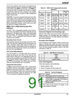
Table 18. IEEE 1149.1 Supported Instruction
Summary
Selected
Data
Description Mode Register
Instruction Instruction
Name
Code
EXTEST
0000
External Test
Test
Normal ID REG
Normal BSR
BSR
CAUTION: To prevent unwanted interrupts from other
active parts of the controller, care must be taken to
mask all likely interruptible events during Magic Packet
mode. An example would be the interrupts from the
Media Independent Interface, which could occur while
the device is in Magic Packet mode.
ID Code
Inspection
IDCODE
0001
Sample
Boundary
SAMPLE
TRIBYP
0010
0011
Force Float Normal Bypass
Control
SETBYP
BYPASS
0100
1111
Boundary to
I/0
Test
Bypass
IEEE 1149.1 (1990) Test Access Port
Interface
Bypass Scan Normal Bypass
An IEEE 1149.1-compatible boundary scan Test Ac-
cess Port is provided for board-level continuity test and
diagnostics. All digital input, output, and input/output
pins are tested. The following paragraphs summarize
the IEEE 1149.1-compatible test functions imple-
mented in the controller.
Instruction Register and Decoding Logic
After the TAP FSM is reset, the IDCODE instruction is
always invoked. The decoding logic gives signals to
control the data flow in the data registers according to
the current instruction.
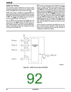
Boundary Scan Circuit
Boundary Scan Register
The boundary scan test circuit requires four pins (TCK,
TMS, TDI, and TDO), defined as the Test Access Port
(TAP). It includes a finite state machine (FSM), an in-
struction register, a data register array, and a power-on
reset circuit. Internal pull-up resistors are provided for
the TDI, TCK, and TMS pins.
Each Boundary Scan Register (BSR) cell has two
stages. A flip-flop and a latch are used for the Serial
Shift Stage and the Parallel Output Stage, respectively.
There are four possible operation modes in the BSR
cell shown in Table 19.
TAP Finite State Machine
Table 19. BSR Mode Of Operation
The TAP engine is a 16-state finite state machine
(FSM), driven by the Test Clock (TCK), and the Test
Mode Select (TMS) pins. An independent power-on
reset circuit is provided to ensure that the FSM is in the
TEST_LOGIC_RESET state at power-up. Therefore,
the TRST is not provided. The FSM is also reset when
TMS and TDI are high for five TCK periods.
1
2
3
4
Capture
Shift
Update
System Function
Other Data Registers
Other data registers are the following:
Supported Instructions
1. Bypass register (1 bit)
In addition to the minimum IEEE 1149.1 requirements
(BYPASS, EXTEST, and SAMPLE instructions), three
additional instructions (IDCODE, TRIBYP, and SET-
BYP) are provided to further ease board-level testing.
All unused instruction codes are reserved. See Table
18 for a summary of supported instructions.
2. Device ID register (32 bits) (Table 20).
Table 20. Device ID Register
Bits 31-28
Bits 27-12
Version
Part Number (0010 0110 0010 0110)
Manufacturer ID. The 11 bit manufacturer ID
cod for AMD is 00000000001 in accordance
with JEDEC publication 106-A.
Bits 11-1
Bit 0
Always a logic 1
Note: The content of the Device ID register is the
same as the content of CSR88.
Am79C978
91

 AMD [ AMD ]