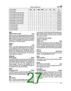
AMD
P R E L I M I N A R Y
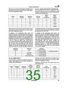
A/D converter. Only one input will be sampled at any
time for conversion by the internal Am79C930 device’s
A/D circuit. The input that will be converted by the
A/D circuit is determined by the setting of the SRCS bit
of the Antenna Diversity and A/D Control register in the
TAI (TIR26).
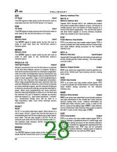
TXMOD
Transmit Modulation Enable
Output
TXMOD is an active low output that is used to enable the
transmit modulation function of the attached trans-
ceiver. Thispinisdirectlycontrolledbythetransmitstate
machine in the TAI and the TXMOD bit of TIR11. The
timing of the TXMOD signal is programmable from a TAI
register. The polarity of this pin is programmable from a
TAI register.
LNK
Link LED
Output
LNK is an active low open collector output that is directly
controllable through a TAI register. This pin is capable of
sinking the 12 mA necessary to drive a typical indicator
LED. This pin is directly controllable through a TAI regis-
ter and is also programmable as an I/O with read capa-
bility. This pin may also be programmed to actively drive
high output values. When an LED is connected to this
pin, then proper operation of this output requires a
pull-up device to be connected externally.
TXPE
Transmit Power Enable
Output
TXPE is an active low output that is used to enable the
transceiver’s transmission amplifier. WhenTXPE is low,
the transceiver should enable its transmission amplifier.
When TXPE is high, the transceiver should disable its
transmission amplifier. This pin is directly controlled by
the transmit state machine in the TAI and theTXPE bit of
the TIR11. The timing of the TXMOD signal is program-
mable from a TAI register. The polarity of this pin is pro-
grammable from a TAI register.
PWRDWN
Powerdown
Output
PWRDWN is an output that becomes active (HIGH)
when the Am79C930 device enters the power down
mode. This pin can be used to power down other sec-
tions of a Am79C930-based system design.
USER7
USER7
Input/Output
USER7 is a pin that may be directly controlled through
TIR and TCR register locations.
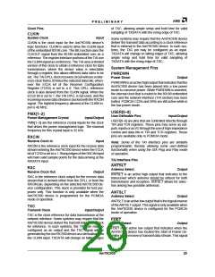
SAR[6–0]
Serial Approximation Register
Input/Output
Other Pins
SAR[6–0] are outputs that are used to deliver the value
of the internal A/D converter for use external to the
Am79C930 device. These pins are directly controllable
through a TAI register and are also programmable as
I/O pins with read capability.
ACT
Activity LED
Output
ACT is an active low open collector output that is directly
controllable through a TAI register. This pin is capable of
sinking the 12 mA necessary to drive a typical indicator
LED. This pin is directly controllable through a TAI regis-
ter and is also programmable as an I/O with read capa-
bility. This pin may also be programmed to actively drive
high output values. When an LED is connected to this
pin, then proper operation of this output requires a
pull-up device to be connected externally.
SDCLK
Serial Device Clock
Output
SDCLK is an output that is used to clock data on the
SDDATA output pin. This pin may be used in combina-
tion with the SDDATA andSDSEL output pins in order to
create an I2C serial device interface. This pin is directly
controllable through a TAI register and is also program-
mable as an I/O with read capability.
ADREF
A/D Reference
Input
ADREF is a single-ended analog input that is used by
the A/D conversion circuit. ADREF is the reference volt-
age that is fed to the resistor ladder of the D/A portion of
the A/D circuit. ADREF is used to determine the range of
sensitivity of the A/D circuit. The recommended value
for ADREF is 1.25 to 1.75 V. Note that ADREF is volt-
age-doubled before being used for internal A/D refer-
ence. For example, an ADREF value of 1.75 V will mean
that the A/D will give a max digital output value for an
ADIN input of 3.5 V or higher.
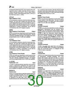
SDDATA
Serial Device Data
Input/Output
SDDATA is an I/O pin that may be used in conjunction
with the SDCLK and SDSEL pins in order to create an
I2C serial device interface. This pin is directly controlla-
ble through a TAI register and is also programmable as
an I/O with read capability.
SDSEL[1–3]
Serial Device Select
Output
SDSEL[1–3] are output pins that may be used in con-
junctionwiththeSDCLKandSDSEL pinsinordertocre-
ate an I2C serial device interface. These pins are directly
controllable through a TAI register and are also pro-
grammable as I/O pins with read capability.
ADIN[1–2]
A/D sample inputs
Input/Output
ADIN[1–2] are inputs that accept single-ended analog
input values for conversion by the internal Am79C930
Am79C930
31

 AMD [ AMD ]