AMD
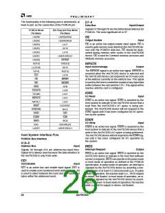
D7–0
P R E L I M I N A R Y
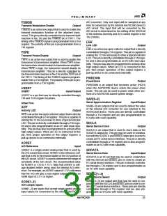
Function Mode
REG
CE1
H
L
IORD IOWR
A0
X
L
OE
X
L
WE
X
Standby mode
X
H
H
H
H
L
X
H
H
H
H
H
H
H
H
L
X
H
H
H
H
H
H
H
H
H
H
L
High-Z
Common Memory Read Even Byte
Common Memory Read Odd Byte
Common Memory Write Even Byte
Common Memory Write Odd Byte
Attribute Memory Read Even Byte
Attribute Memory Read Odd Byte
Attribute Memory Write Even Byte
Attribute Memory Write Odd Byte
I/O Read Even Byte
H
H
L
Even Byte
Odd Byte
Even Byte
Odd Byte
Even Byte
Odd Byte
Even Byte
Odd Byte
Even Byte
Odd Byte
Even Byte
Odd Byte
L
H
L
L
L
H
H
L
L
H
L
L
L
H
H
L
L
L
H
L
L
L
L
H
H
H
H
H
H
L
L
H
L
L
L
L
H
H
H
H
I/O Read Odd Byte
L
L
L
H
L
I/O Write Even Byte
L
L
H
H
I/O Write Odd Byte
L
L
L
H
device from the PCMCIA data bus. WE should be deas-
serted during memory read cycles to the Am79C930.
WE is used for Common memory accesses and Attrib-
ute memory accesses.
REG
Attribute Memory Select
Input
REG is an active low-input signal that selects among At-
tributememoryandCommonmemoryintheAm79C930
device and the Am79C930-based PCMCIA card. When
REG is asserted, then the current access is to Attribute
memory or I/O. When REG is not asserted, then the cur-
rent access is to Common memory.
ISA (IEEE P996) Bus interface
LA23–17, SA16–0
Address Bus
Input
Signals SA0 through SA16 and LA17 through LA23
areaddress-bus-inputlineswhichenabledirectaddress
of up to 16 Mbytes of memory space in an ISA-based
Am79C930design. SignalSA0isalwaysused, because
the data interface to the Am79C930 is only 8-bits wide.
RESET
Reset
Input
RESET is an active high-input signal that clears the
Card Configuration Option Register CCOR) and places
the Am79C930 device into an unconfigured (PCMCIA-
Memory-Only Interface) state. This pin also causes a
RESET to be asserted to each of the Am79C930 core
function units (i.e., PCMCIA interface, CPU, and Trans-
ceiver Attachment Interface).
SD7–0
Data Bus
Input/Output
Signals SD7 through SD0 are the bidirectional data bus
for ISA. The most significant bit is SD7.
AEN
Address Enable
STSCHG
Status Change
Input
Output
AEN is driven LOW by the ISA host to indicate when an
I/O address is valid.
TheSTSCHG signal is an active low signal.STSCHG as
implemented in the Am79C930 device is only used for
the PCMCIA WAKEUP indication. The CHANGED bit
and the SIGCHG bit of the Card Configuration and
Status Register (CCSR) are not supported by the
Am79C930 device. The Pin Replacement Register is
not supported by the Am79C930 device.
BALE
Bus Address Latch Enable
Input
BALE is driven by the ISA host to indicate when the ad-
dress signal lines are valid.
WAIT
Extend Bus Cycle
IOCHRDY
I/O Channel Ready
Output
Output
The WAIT signal is an active low signal. WAIT is as-
serted by the Am79C930 device to delay completion of
the access cycle currently in progress.
The IOCHRDY signal is deasserted by the Am79C930
device at the beginning of a memory access in order
to delay completion of the memory access cycle then
in progress. The IOCHRDY signal is reasserted by
the Am79C930 device when the memory access
is completed.
WE
Write Enable
Input
WE is an active low write-enable input signal. WE is
used to strobe memory write data into the Am79C930
Am79C930
27

 AMD [ AMD ]