AMD
P R E L I M I N A R Y
for an output function. This means that there are con-
figurations for which a read of the pin data register bit will
not reflect what has most recently been written to the pin
data register bit ( i.e., if a pin is configured as an output
with its data source as some internal circuit, then the
user may write the pin data bit with a given value, and a
read of this same bit will yield the output function value,
which may not necessarily match the value just written
to the data bit). This functionality is given as a note
following each table. Also note that for a few pins,
the read and write locations for the pin data are in
different places.
Note that a read of the USERDT[4] bit (TIR29[4]) will al-
ways give the current USER4/LA17 pin value, regard-
less of pin configuration setting.
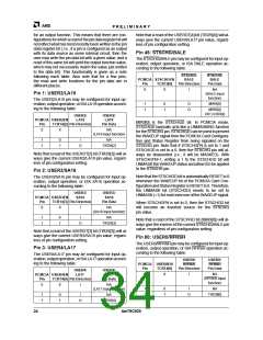
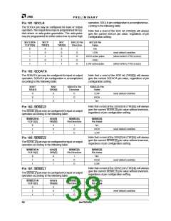
Pin 45: STSCHG/BALE
The STSCHG/BALE pin may be configured for input op-
eration, output operation, or ISA BALE operation ac-
cording to the following table:
STSCHG/
BALE
STSCHG/
BALE
PCMCIA STSCHGFN
Pin
TCR15[0]
Pin Direction
Pin Data
0
X
I
NA
Pin 1: USER2/LA19
(BALE input
function)
The USER2/LA19 pin may be configured for input op-
eration, outputoperation, orISALA19operationaccord-
ing to the following table:
1
1
0
1
O
O
MIR9[0]
MIR9[0]
OR CCSR[4]
USER2/
LA19
USER2/
LA19
PCMCIA USER2EN
MIR9[0] is the STSCHGD bit. In PCMCIA mode,
STSCHGD basically acts like a UNMASKING function
for the STSCHG pin. STSCHGD can be used to prevent
the WAKEUP signal from the PCMCIA Card Configura-
tion and Status Register from being signaled on the
STSCHG pin. Note that if STSCHGFN is set to 1 and
STSCHGD is set to a 0, then the STSCHG pin will al-
ways be deasserted (i.e., it will be MASKED). With
STSCHGFN=1, writing a 1 to the STSCHGD bit will
UNMASK the WAKEUP status and allow it to be applied
to the STSCHG pin.
Pin
TCR14[2] Pin Direction
Pin Data
0
X
I
NA
(LA19 input function)
1
1
0
1
I
NA
O
TIR29[2]
Note that a read of the USERDT[2] bit (TIR29[2]) will al-
ways give the current USER2/LA19 pin value, regard-
less of pin configuration setting.
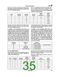
Pin 2: USER3/SA16
Note that the STSCHGD bit is automatically RESET to 0
whenever the WAKEUP bit of the PCMCIA Card Con-
figuration and Status Register is RESET to 0. Therefore,
the UNMASK bit (STSCHGD) needs to be set to
UNMASK (=1) for each new use of the WAKEUP signal.
The USER3/SA16 pin may be configured for input op-
eration, output operation, or ISA SA16 operation ac-
cording to the following table:
USER3/
SA16
USER3/
SA16
PCMCIA USER3EN
Pin
TCR14[3] Pin Direction
Pin Data
When STSCHGFN is set to 0, then the STSCHGD bit
will become an inverted source for the STSCHG
pin value.
0
X
I
NA
(SA16 input function)
1
1
0
1
I
NA
Note that a read of the STSCHGD bit (MIR9[0]) will al-
ways give the inverse of the current STSCHG/BALE pin
value, regardless of pin configuration setting.
O
TIR29[3]
Note that a read of the USERDT[3] bit (TIR29[3]) will al-
ways give the current USER3/SA16 pin value, regard-
less of pin configuration setting.
Pin 90: USER0/RFRSH
The USER0/RFRSH pin may be configured for input op-
eration, output operation, or ISA RFRSH operation ac-
cording to the following table:
Pin 3: USER4/LA17
The USER4/LA17 pin may be configured for input op-
eration, outputoperation, orISALA17operationaccord-
ing to the following table:
USER0/
RFRSH
Pin Direction
USER0/
RFRSH
Pin Data
PCMCIA USER0EN
Pin
TCR14[0]
USER4/
LA17
USER4/
LA17
0
X
I
NA
PCMCIA USER4EN
(RFRSH input
function)
Pin
TCR14[4] Pin Direction
Pin Data
0
X
I
NA
1
1
0
1
I
NA
(LA17 input function)
O
TIR29[0]
1
1
0
1
I
NA
O
TIR29[4]
34
Am79C930

 AMD [ AMD ]