AMD
P R E L I M I N A R Y
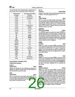
Memory Interface Pins
IOR
I/O Read
Input
MA16–0
Memory Address Bus
The IOR signal is made active by the ISA host in order to
Output
read data from the Am79C930 device’s I/O space.
Signals MA0 through MA16 are address-bus-output
lines which enable direct address of up to 128 Kbytes of
SRAM memory and 128 Kbytes of Flash memory in a
Am79C930-based application. The Am79C930 device
will drive these signals to Access memory locations
within the SRAM or the Flash memory.
IOW
I/O Write
Input
TheIOW signalismadeactivebytheISAhostinorderto
write data to the Am79C930 device’s I/O space.
MEMR
Memory Read
FCE
Input
Flash Memory Chip Enable
Output
The MEMR signal is made active by the ISA host in
order to read data from the Am79C930 device’s
memory space.
FCE is an active low chip enable output signal. FCE is
used to activate the Flash memory device’s control logic
and input buffers during accesses on the memory
interface bus.
MEMW
Memory Write
Input
MD7–0
Memory Data Bus
Input/Output
The MEMW signal is made active by the ISA host in
order to write data to the Am79C930 device’s
memory space.
Signals MD7 through MD0 are the bidirectional data bus
for the SRAM and the Flash memory. The most signifi-
cant bit is MD7.
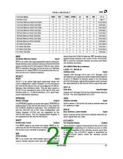
IRQ[4,5,9–12]
Interrupt Request
Output
MOE
Memory Output Enable
Output
IRQ[x] is asserted by the Am79C930 device to indicate
to the host that software service is required. IRQ[x] is
held at the inactive level when no interrupt is requested.
Only one of the six IRQ[x] lines may be selected for use
at any one time. IRQ[x] outputs may be programmed for
edge or level operation. Edge or level programming is
part of the ISA Plug and Play initialization procedure.
When edge programming has been selected, then the
selected IRQ[x] pin is driven to a HIGH level to indicate
an active interrupt request, and the selected IRQ[x] pin
is driven to a low level to indicate an inactive interrupt re-
quest. When level programming has been selected,
then the selected IRQ[x] pin is driven to a LOW level and
the selected IRQ pin is floated to indicate an inactive
interrupt request (i.e., open drain operation). “Unused”
(i.e., unselected) IRQ[x] lines will be held in a
high impedance state, even when interrupt service
is requested.
MOE is an active low output that is used to gate the out-
puts of the SRAM and Flash memory device’s during
read cycles.
SCE
SRAM Chip Enable
Output
SCE is an active low chip enable output signal. SCE
is used to activate the SRAM device’s control logic and
input buffers during accesses on the memory
interface bus.
MWE
Memory Write Enable
Output
MWE isanactivelowoutputthatisusedtolatchaddress
and data information in the SRAM and Flash memory
devices during write cycles. Address information for
SRAM and Flash memory write cycles is valid on the
MA16–0 pins at the falling edge of MWE. Data informa-
tion for SRAM and Flash memory write cycles is valid on
the MD7–0 pins at the rising edge of MWE.
RESET
Reset
Input
RESET is an active high input signal. When driven to a
HIGH level, RESET causes the Am79C930 device to
immediately place all ISA bus outputs into a high imped-
ance state. This pin also causes a RESET to be as-
serted to each of the Am79C930 core function units (i.e.,
ISA interface state machine, 80188, and Transceiver
Attachment Interface).
XCE
eXtra Chip Enable
Output
XCE is an active low chip enable output signal. XCE is
used to activate a peripheral device’s control logic and
input buffers during accesses on the memory interface
bus. XCE is activated by appropriate signaling from the
80188 embedded core. XCE may not be activated
through the system interface. Sixteen bytes of address
range are allotted for use with the XCE signal.
RFRSH
Refresh
Input
The RFRSH signal is made active by the ISA host to in-
dicate that the current bus cycle is a refresh operation.
28
Am79C930

 AMD [ AMD ]