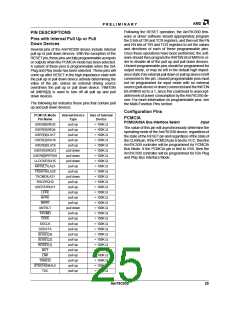
AMD
P R E L I M I N A R Y
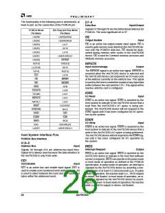
Clock Pins
of TXC, allowing ample setup and hold time for valid
sampling of TXDATA with the rising edge of TXC.
CLKIN
System Clock
Input
Some systems may require that the Am79C930 device
deliver the transmit data according to a clock reference
that is external to the Am79C930 device. In such sys-
tems, the TXC pin may be configured as an input.
TXDATA will change on falling edges of TXC, allowing
ample setup and hold time for valid sampling of
TXDATA with the rising edge of TXC.
CLKIN is the clock input for the Am79C930 device’s
logic functions. CLKIN is used to drive the CLKIN input
of the embedded 80188 core. The BIU section uses the
CLKOUT signal from the 80188 embedded core as a
reference. The register interface portions of the TAI use
the CLKIN signal as a reference. The TAI uses a divided
version of this clock to obtain a reference clock for data
transmission, where the divisor value is selectable
through a register; this allows different data rates to be
set. The TAI DPLL clock recovery circuit will use a refer-
ence clock that is 20 times the selected data rate, when-
ever the ECLK bit of the Receiver Configuration
Register (TCR3) is set to a 0. This DPLL reference
clock is also derived from the CLKIN signal. When the
ECLK bit is set to 1, the TAI DPLL is not used, and the
incoming receive data stream is clocked with the RXCIN
signal. The highest frequency allowed at the CLKIN in-
put is 40 MHz.
System Management Pins
PWRDWN
Power Down
Output
PWRDWN is an active high output that indicates that the
Am79C930 device has been placed into a low power
mode to conserve power. While PWRDWN is asserted,
the internal clock that is routed to the 80188 embedded
core and the network interface (TAI section) has been
halted. PCMCIA CCRs and SIRs are still active while in
the low power mode.
USER[0–6]
User-Definable Pins
PMX[1–2]
Power Management Crystal
Input/Output
Input/Output
USER[0–6] are pins that are controlled directly through
TIR and TCR registers. These pins may serve as out-
puts, inputs or as I/O through the use of high-impedance
control and data bits in TIR and TCR registers. These
pins are available only in PCMCIA mode.
PMX[1–2] are the reference crystal inputs for the clock
that drives the power management logic. The nominal
frequency for this crystal input is 32 kHz.
RXCIN
Receive Clock In
Input
Note: Some of the TAI interface pins are similarly
programmable, thereby allowing some user-defined
functionality when using the ISA Plug and Play mode
of operation.
RXCIN is the reference clock input for the receive data
stream entering the Am79C930 device when the ECLK
bit of TCR2 is set to a 1. Rising edges of the RXCIN input
will mark valid sample points for the data arriving at the
RXDATA input.
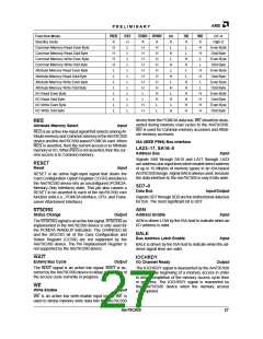
TAI Interface Pins
ANTSLT
RXC
Antenna Select
Output
Receive Clock Out
Output
ANTSLT is an active high output that indicates to the
transceiver which antenna should be utilized for both
transmission and reception. ANTSLT allows for selec-
tion among two possible antennas.
RXC is the reference clock output for the receive data
stream that is derived either from the DPLL or from the
RXCIN pin, depending on the selected Am79C930 de-
vice configuration. This clock is provided for test pur-
poses only. This function is only available when the
Am79C930 device is programmed for the PCMCIA
mode of operation.
ANTSLT
Antenna Select
Output
ANTSLTisanactivelowoutputthatisthelogicalinverse
of the ANTSLT output. This signal is only available when
the Am79C930 device is configured for the PCMCIA
mode of operation.
TXC
Transmit Clock
Input/Output
TXC is the clock reference for data transmission at the
network interface. Some systems may require that the
Am79C930 device deliver the transmit data with a clock
for reference. In such systems, the TXC pin may be
configured as an output and the TXC signal will be
generatedbytheAm79C930deviceasaderivativefrom
the CLKIN input. TXDATA will change on falling edges
FDET
Frame Detect
Output
FDET is an active low output that indicates when the
Am79C930 device has located the Start of Frame De-
limiter in the receive or transmit data stream. This signal
Am79C930
29

 AMD [ AMD ]