D A T A S H E E T
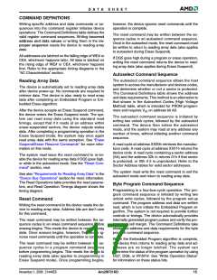
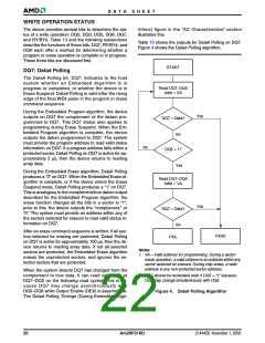
Any commands written to the device during the Em-
bedded Program Algorithm are ignored. Note that a
hardware reset immediately terminates the program-
ming operation. The program command sequence
should be reinitiated once the device has reset to read-
ing array data, to ensure data integrity.
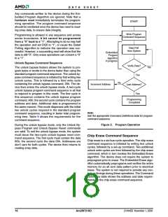
START
Write Program
Command Sequence
Programming is allowed in any sequence and across
sector boundaries. A bit cannot be programmed
from a “0” back to a “1”. Attempting to do so may halt
the operation and set DQ5 to “1”, or cause the Data#
Polling algorithm to indicate the operation was suc-
cessful. However, a succeeding read will show that the
data is still “0”. Only erase operations can convert a “0”
to a “1”.
Data Poll
from System
Embedded
Program
algorithm
in progress
Unlock Bypass Command Sequence
Verify Data?
Yes
No
The unlock bypass feature allows the system to pro-
gram bytes or words to the device faster than using the
standard program command sequence. The unlock by-
pass command sequence is initiated by first writing two
unlock cycles. This is followed by a third write cycle
containing the unlock bypass command, 20h. The de-
vice then enters the unlock bypass mode. A two-cycle
unlock bypass program command sequence is all that
is required to program in this mode. The first cycle in
this sequence contains the unlock bypass program
command, A0h; the second cycle contains the program
address and data. Additional data is programmed in
the same manner. This mode dispenses with the initial
two unlock cycles required in the standard program
command sequence, resulting in faster total program-
ming time. Table 9 shows the requirements for the
command sequence.
No
Increment Address
Last Address?
Yes
Programming
Completed
Note:
See the appropriate Command Definitions table for program
command sequence.
Figure 2. Program Operation
During the unlock bypass mode, only the Unlock By-
pass Program and Unlock Bypass Reset commands
are valid. To exit the unlock bypass mode, the system
must issue the two-cycle unlock bypass reset com-
mand sequence. The first cycle must contain the data
90h; the second cycle the data 00h. Addresses are
don’t care for both cycles. The device then returns to
reading array data.
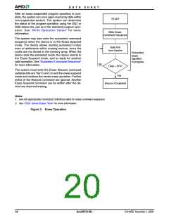
Chip Erase Command Sequence
Chip erase is a six-bus-cycle operation. The chip erase
command sequence is initiated by writing two unlock
cycles, followed by a set-up command. Two additional
unlock write cycles are then followed by the chip erase
command, which in turn invokes the Embedded Erase
algorithm. The device does not require the system to
preprogram prior to erase. The Embedded Erase algo-
rithm automatically preprograms and verifies the entire
memory for an all zero data pattern prior to electrical
erase. The system is not required to provide any con-
trols or timings during these operations. The Command
Definitions table shows the address and data require-
ments for the chip erase command sequence.
16
Am29F016D
21444E6 November 1, 2006

 AMD [ AMD ]