D A T A S H E E T
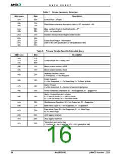
Table 7. Device Geometry Definition
Addresses
Data
Description
27h
15h
Device Size = 2N byte
28h
29h
00h
00h
Flash Device Interface description (refer to CFI publication 100)
2Ah
2Bh
00h
00h
Max. number of byte in multi-byte write = 2N
(00h = not supported)
2Ch
01h
Number of Erase Block Regions within device
2Dh
2Eh
2Fh
30h
1Fh
00h
00h
01h
Erase Block Region 1 Information
(refer to the CFI specification or CFI publication 100)
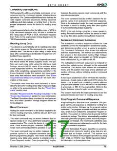
Table 8. Primary Vendor-Specific Extended Query
Data Description
Addresses
40h
41h
42h
50h
52h
49h
Query-unique ASCII string “PRI”
43h
44h
31h
31h
Major version number, ASCII
Minor version number, ASCII
Address Sensitive Unlock
0 = Required, 1 = Not Required
45h
46h
00h
02h
Erase Suspend
0 = Not Supported, 1 = To Read Only, 2 = To Read & Write
Sector Protect
0 = Not Supported, X = Number of sectors in per group
47h
48h
04h
01h
Sector Temporary Unprotect: 00 = Not Supported, 01 = Supported
Sector Protect/Unprotect scheme
49h
04h
01 = 29F040 mode, 02 = 29F016 mode,
03 = 29F400 mode, 04 = 29LV800A mode
4Ah
4Bh
00h
00h
Simultaneous Operation: 00 = Not Supported, 01 = Supported
Burst Mode Type: 00 = Not Supported, 01 = Supported
Page Mode Type: 00 = Not Supported, 01 = 4 Word Page,
02 = 8 Word Page
4Ch
00h
4Dh
4Eh
00h
00h
ACC supply minimum
ACC supply maximum
Top/bottom boot sector flag
2 = bottom, 3 = top. If address 2Ch = 01h, ignore this field
4Fh
00h
14
Am29F016D
21444E6 November 1, 2006

 AMD [ AMD ]