D A T A S H E E T
The system can read CFI information at the addresses
given in Tables 5–8. To terminate reading CFI data, the
system must write the reset command.
COMMON FLASH MEMORY INTERFACE
(CFI)
The Common Flash Interface (CFI) specification out-
lines device and host system software interrogation
handshake, which allows specific vendor-specified
software algorithms to be used for entire families of de-
vices. Software support can then be device-
independent, JEDEC ID-independent, and forward-
and backward-compatible for the specified flash device
families. Flash vendors can standardize their existing
interfaces for long-term compatibility.
The system can also write the CFI query command
when the device is in the autoselect mode. The device
enters the CFI query mode, and the system can read
CFI data at the addresses given in Tables 5–8. The sys-
tem must write the reset command to return the device
to the autoselect mode.
For further information, please refer to the CFI Specifi-
cation and CFI Publication 100, available via the World
Wide Web at http://www.amd.com/products/nvd/over-
view/cfi.html. Alternatively, contact an AMD
representative for copies of these documents.
This device enters the CFI Query mode when the sys-
tem writes the CFI Query command, 98h, to address
55h, any time the device is ready to read array data.
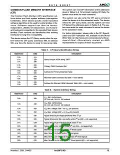
Table 5. CFI Query Identification String
Description
Addresses
Data
10h
11h
12h
51h
52h
59h
Query Unique ASCII string “QRY”
Primary OEM Command Set
13h
14h
02h
00h
15h
16h
40h
00h
Address for Primary Extended Table
17h
18h
00h
00h
Alternate OEM Command Set (00h = none exists)
Address for Alternate OEM Extended Table (00h = none exists)
19h
1Ah
00h
00h
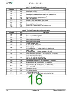
Table 6. System Interface String
Description
Addresses
Data
VCC Min. (write/erase)
D7–D4: volt, D3–D0: 100 millivolt
1Bh
45h
VCC Max. (write/erase)
D7–D4: volt, D3–D0: 100 millivolt
1Ch
55h
1Dh
1Eh
1Fh
20h
21h
22h
23h
24h
25h
26h
00h
00h
03h
00h
0Ah
00h
05h
00h
04h
00h
VPP Min. voltage (00h = no VPP pin present)
VPP Max. voltage (00h = no VPP pin present)
Typical timeout per single byte/word write 2N µs
Typical timeout for Min. size buffer write 2N µs (00h = not supported)
Typical timeout per individual block erase 2N ms
Typical timeout for full chip erase 2N ms (00h = not supported)
Max. timeout for byte/word write 2N times typical
Max. timeout for buffer write 2N times typical
Max. timeout per individual block erase 2N times typical
Max. timeout for full chip erase 2N times typical (00h = not supported)
November 1, 2006 21444E6
Am29F016D
13

 AMD [ AMD ]