D A T A S H E E T
Command Definitions
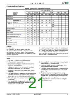
Table 9. Am29F016D Command Definitions
Bus Cycles (Notes 2–4)
Command
Sequence
(Note 1)
First
Second
Third
Addr
Fourth
Data Addr Data
Fifth
Sixth
Addr Data Addr Data
Addr Data Addr Data
Read (Note 5)
Reset (Note 6)
Manufacturer ID
1
1
4
4
RA
RD
F0
XXX
555
555
AA
AA
2AA
2AA
55
55
555
555
90
90
X00
X01
01
Autoselect
Device ID
AD
(Note 7)
XX00
XX01
Sector Group Protect
Verify (Note 8)
SGA
X02
4
555
AA
2AA
55
555
90
CFI Query (Note 9)
Program
1
4
3
2
2
6
6
1
1
55
98
AA
AA
A0
90
AA
AA
B0
30
555
555
XXX
XXX
555
555
XXX
XXX
2AA
2AA
PA
55
55
PD
00
55
55
555
555
A0
20
PA
PD
Unlock Bypass
Unlock Bypass Program (Note 10)
Unlock Bypass Reset (Note 11)
Chip Erase
XXX
2AA
2AA
555
555
80
80
555
555
AA
AA
2AA
2AA
55
55
555
SA
10
30
Sector Erase
Erase Suspend (Note 9)
Erase Resume (Note 10)
Legend:
X = Don’t care
PD = Data to be programmed at location PA. Data latches on
the rising edge of WE# or CE# pulse, whichever happens first.
RA = Address of the memory location to be read.
SA = Address of the sector to be verified (in autoselect mode)
or erased. Address bits A20–A16 select a unique sector.
RD = Data read from location RA during read operation.
PA = Address of the memory location to be programmed.
Addresses latch on the falling edge of the WE# or CE# pulse,
whichever happens later.
SGA = Address of the sector group to be verified. Address bits
A20–A18 select a unique sector group.
Notes:
1. See Table 1 for description of bus operations.
2. All values are in hexadecimal.
9. Command is valid when device is ready to read array data
or when device is in autoselect mode.
3. Except when reading array or autoselect data, all bus
cycles are write operations.
10. The Unlock Bypass command is required prior to the
Unlock Bypass Program command.
4. Address bits A20–A11 are don’t cares for unlock and
command cycles, unless SA or PA required.
11. The Unlock Bypass Reset command is required to return
to reading array data when the device is in the unlock
bypass mode.
5. No unlock or command cycles required when reading
array data.
12. The system may read and program in non-erasing
sectors, or enter the autoselect mode, when in the Erase
Suspend mode. The Erase Suspend command is valid
only during a sector erase operation.
6. The Reset command is required to return to reading array
data when device is in the autoselect mode, or if DQ5
goes high (while the device is providing status data).
7. The fourth cycle of the autoselect command sequence is
a read cycle.
13. The Erase Resume command is valid only during the
Erase Suspend mode.
8. The data is 00h for an unprotected sector group and 01h
for a protected sector group.See “Autoselect Command
Sequence” for more information.
November 1, 2006 21444E6
Am29F016D
19

 AMD [ AMD ]