D A T A S H E E T
WRITE OPERATION STATUS
The device provides several bits to determine the sta-
tus of a write operation: DQ2, DQ3, DQ5, DQ6, DQ7,
and RY/BY#. Table 10 and the following subsections
describe the functions of these bits. DQ7, RY/BY#, and
DQ6 each offer a method for determining whether a
program or erase operation is complete or in progress.
These three bits are discussed first.
rithms) figure in the “AC Characteristics” section
illustrates this.
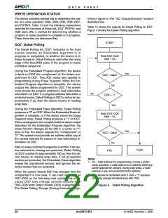
Table 10 shows the outputs for Data# Polling on DQ7.
Figure 4 shows the Data# Polling algorithm.
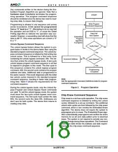
START
DQ7: Data# Polling
The Data# Polling bit, DQ7, indicates to the host
system whether an Embedded Algorithm is in
progress or completed, or whether the device is in
Erase Suspend. Data# Polling is valid after the rising
edge of the final WE# pulse in the program or erase
command sequence.
Read DQ7–DQ0
Addr = VA
During the Embedded Program algorithm, the device
outputs on DQ7 the complement of the datum pro-
grammed to DQ7. This DQ7 status also applies to
programming during Erase Suspend. When the Em-
bedded Program algorithm is complete, the device
outputs the datum programmed to DQ7. The system
must provide the program address to read valid status
information on DQ7. If a program address falls within a
protected sector, Data# Polling on DQ7 is active for ap-
proximately 2 µs, then the device returns to reading
array data.
Yes
DQ7 = Data?
No
No
DQ5 = 1?
Yes
During the Embedded Erase algorithm, Data# Polling
produces a “0” on DQ7. When the Embedded Erase al-
gorithm is complete, or if the device enters the Erase
Suspend mode, Data# Polling produces a “1” on DQ7.
This is analogous to the complement/true datum output
described for the Embedded Program algorithm: the
erase function changes all the bits in a sector to “1”;
prior to this, the device outputs the “complement,” or
“0.” The system must provide an address within any of
the sectors selected for erasure to read valid status in-
formation on DQ7.
Read DQ7–DQ0
Addr = VA
Yes
DQ7 = Data?
No
After an erase command sequence is written, if all sec-
tors selected for erasing are protected, Data# Polling
on DQ7 is active for approximately 100 µs, then the de-
vice returns to reading array data. If not all selected
sectors are protected, the Embedded Erase algorithm
erases the unprotected sectors, and ignores the se-
lected sectors that are protected.
PASS
FAIL
Notes:
1. VA = Valid address for programming. During a sector
erase operation, a valid address is an address within any
sector selected for erasure. During chip erase, a valid
address is any non-protected sector address.
When the system detects DQ7 has changed from the
complement to true data, it can read valid data at
DQ7–DQ0 on the following read cycles. This is be-
cause DQ7 may change asynchronously with
DQ0–DQ6 while Output Enable (OE#) is asserted low.
The Data# Polling Timings (During Embedded Algo-
2. DQ7 should be rechecked even if DQ5 = “1” because
DQ7 may change simultaneously with DQ5.
Figure 4. Data# Polling Algorithm
20
Am29F016D
21444E6 November 1, 2006

 AMD [ AMD ]