D A T A S H E E T
the device immediately terminates any operation in
Program and Erase Operation Status
progress, tristates all data output pins, and ignores all
read/write attempts for the duration of the RESET#
pulse. The device also resets the internal state ma-
chine to reading array data. The operation that was
interrupted should be reinitiated once the device is
ready to accept another command sequence, to en-
sure data integrity.
During an erase or program operation, the system may
check the status of the operation by reading the status
bits on DQ7–DQ0. Standard read cycle timings and I
CC
read specifications apply. Refer to “Write Operation
Status” for more information, and to each AC Charac-
teristics section for timing diagrams.
Standby Mode
Current is reduced for the duration of the RESET#
pulse. When RESET# is held at V , the device enters
IL
When the system is not reading or writing to the device,
it can place the device in the standby mode. In this
mode, current consumption is greatly reduced, and the
outputs are placed in the high impedance state, inde-
pendent of the OE# input.
the TTL standby mode; if RESET# is held at V
SS
0.5 V, the device enters the CMOS standby mode.
The RESET# pin may be tied to the system reset cir-
cuitry. A system reset would thus also reset the Flash
memory, enabling the system to read the boot-up firm-
ware from the Flash memory.
The device enters the CMOS standby mode when CE#
and RESET# pins are both held at V
0.5 V. (Note
CC
that this is a more restricted voltage range than V .)
The device enters the TTL standby mode when CE#
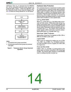
If RESET# is asserted during a program or erase oper-
ation, the RY/BY# pin remains a “0” (busy) until the
internal reset operation is complete, which requires a
IH
and RESET# pins are both held at V . The device re-
IH
quires standard access time (t ) for read access when
time of t
(during Embedded Algorithms). The
CE
READY
the device is in either of these standby modes, before it
is ready to read data.
system can thus monitor RY/BY# to determine whether
the reset operation is complete. If RESET# is asserted
when a program or erase operation is not executing
(RY/BY# pin is “1”), the reset operation is completed
The device also enters the standby mode when the RE-
SET# pin is driven low. Refer to the next section,
“RESET#: Hardware Reset Pin”.
within a time of t
(not during Embedded Algo-
READY
rithms). The system can read data t
after the
RH
If the device is deselected during erasure or program-
ming, the device draws active current until the
operation is completed.
RESET# pin returns to V .
IH
Refer to the AC Characteristics tables for RESET# pa-
rameters and timing diagram.
In the DC Characteristics tables, I
standby current specification.
represents the
CC3
Output Disable Mode
When the OE# input is at V , output from the device is
disabled. The output pins are placed in the high imped-
ance state.
IH
RESET#: Hardware Reset Pin
The RESET# pin provides a hardware method of reset-
ting the device to reading array data. When the system
drives the RESET# pin low for at least a period of t
,
RP
November 1, 2006 21444E6
Am29F016D
9

 AMD [ AMD ]