Revision 1.02 – April 12, 2007
S5920 – PCI Product: Pass-Thru Operation
Data Book
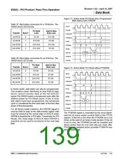
Figure 71. Active mode PCI Read (Zero Programmed
Wait States) with PTADR#
1
2
3
4
5
6
7
Table 57. Big Endian conversion for a 16-bit bus. The
S5920 drives D[15:0] only
ADCLK
PTATN#
PTBURST#
PTNUM[1:0]
PTWR
PCI Byte
Lane
Add-On Bus
Byte Lane
Transfer
1st XFER
1st XFER
2nd XFER
2nd XFER
Byte #
0
1
2
3
D7-D0
D15-D8
D23-D16
D31-D24
D15-D8
D7-D0
D15-D8
D7-D0
01b
PTBE[3:0]
DXFR#
0h
Fh
DQ[31:0]
PTWAIT#
PTADR#
PTADDR
DATA
Table 58. Big Endian conversion for an 8-bit bus. The
S5920 drives D[7:0] only
PCI Byte
Lane
Add-On Bus
Byte Lane
Transfer
1st XFER
2nd XFER
3rd XFER
4th XFER
Byte #
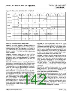
Figure 72. Active Mode PCI Read without PTADR#
0
1
2
3
D7-D0
D15-D8
D23-D16
D31-D24
D7-D0
D7-D0
D7-D0
D7-D0
1
2
3
4
5
6
7
ADCLK
PTATN#
PTBURST#
PTNUM[1:0]
PTWR
01b
0h
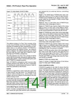
In Active mode, wait states can also be programmed.
This enables easier interfacing to slow Add-On logic
which cannot transfer data at the full ADCLK-
speed.The S5920 inserts a turnaround cycle after the
address phase for PCI Read cycles. If one or more
wait states have been programmed, the turnaround
cycle is considered the first wait state of the first data
phase of that transaction.
PTBE[3:0]
DXFR#
Fh
DQ[31:0]
PTWAIT#
PTADR#
DATA
For all Active mode transfers, the DXFR# signal is
used by Add-On logic as the data transfer signal. Data
must be latched at the rising edge of ADCLK when
DXFR# is asserted for a PCI write. Conversely, for PCI
Reads, the rising edge of ADCLK when DXFR# is
asserted can be used to increment to the next data
field.
The PTADR# signal is controlled by the most signifi-
cant bit of every region control field in the PTCR
register. If this bit is zero then the PTADR# pin is not
driven at the start of an Active mode transfer. If this bit
is set to one, the PTADR# pin will be enabled and
driven active (low) for one and only one clock after
PTATN# was sampled active provided PTWAIT# was
also sampled high.
AMCC Confidential and Proprietary
DS1596
139

 AMCC [ APPLIED MICRO CIRCUITS CORPORATION ]