Revision 1.02 – April 12, 2007
S5920 – PCI Product: Pass-Thru Operation
Data Book
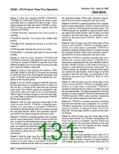
On operation registers, just the APTD register (ADR =
2Ch).
2, PTBE2# is deasserted, and the Add-On may assert
PTRDY#, completing the cycle.
Table 2 shows how the external Add-On data bus is
steered to the Pass-Thru Data Register bytes. This
mechanism is determined by the Pass-Thru region
bus width defined during initialization. The BYTEn
symbols indicate data bytes in the Pass-Thru Data
Register. For example, an 8-bit Add-On write with
BE1# asserted results in the data on DQ[7:0] being
steered into BYTE1 of the APTD register.
Table 54. Byte Lane Steering for PCI Write (Add-On
Read)
Byte
Enables
APTD Register Write Byte Lane
Steering
3
x
x
x
0
2
x
x
0
1
1
x
0
1
1
0
0
1
1
1
DQ[31:24]
BYTE3
BYTE3
BYTE3
BYTE3
DQ[23:16]
BYTE2
BYTE2
BYTE2
BYTE3
DQ[15:8]
BYTE1
BYTE1
BYTE2
BYTE3
DQ[7:0]
BYTE0
BYTE1
BYTE2
BYTE3
To write data into the APTD Register, PTBEn# and
BEn# must both be asserted. The following describes
how APTD writes are controlled:
Write BYTE3 if PTBE3# AND BE3# are asserted
Write BYTE2 if PTBE2# AND BE2# are asserted
Write BYTE1 if PTBE1# AND BE1# are asserted
Write BYTE0 if PTBE0# AND BE0# are asserted
Table 55. Byte Lane Steering for PCI Read (Add-On
Write)
After each byte is written into the Pass-Thru data reg-
ister, its corresponding PTBE[3:0]# output is
deasserted. This allows Add-On logic to monitor which
bytes have been written, and which bytes remain to be
written. When all requested bytes have been written
(all PTBE[3:0]#s are deasserted), PTRDY# is asserted
by the Add-On, completing the access.
Defined PT
Bus Width
APTD Register Write Byte Lane
Steering
BYTE3
DQ[31:24]
DQ[15:8]
DQ[7:0]
BYTE2
BYTE1
BYTE0
DQ[7:0]
DQ[7:0]
DQ[7:0]
32 Bit Data Bus
16 Bit Data Bus
8 Bit Data Bus
DQ[23:16]
DQ[7:0]
DQ[7:0]
DQ[15:8]
DQ[15:8]
DQ[7:0]
There are two methods of accessing the Add-On
Pass-Thru Address Register (APTA): by asserting the
PTADR# pin (and getting the address on DQ after
some propagation delay) or by asserting RD#,
SELECT, BE[3:0]#’s, and ADR[6:2] = 28h (and getting
the address on DQ one cycle later). When using the
PTADR# input, all 32 bits of address are driven on DQ,
regardless of the state of the DQMODE pin. When
accessing APTA via an Add-On operation register
access, all 32 bits of address are driven on DQ as long
as DQMODE indicates 32 bits. If DQMODE is set for
16 bits, it is necessary to perform two accesses: one
with BE[3]# low for the lower 16 bits, and one with
BE[3]# high for the upper 16 bits. The Pass-Thru
region bus-sizes have no effect on APTA accesses.
For Pass-Thru writes (Add-On APTD reads), Add-On
logic must read the APTD register one byte or one
word at a time (depending on the Add-On bus width).
The internal data bus is steered from the correct por-
tion of APTD using the BE[3:0]# inputs. Table 1 shows
the byte lane steering mechanism used by the S5920.
The BYTEn symbols indicate data bytes in the Pass-
Thru Data Register.
When a read by the Add-On is performed with a BEn#
input asserted, the corresponding PTBEn# output is
deasserted. Add-On logic cycles through the byte
enables to read the entire APTD Register. Once all
data is read (all PTBE[3:0]#s are deasserted),
PTRDY# is asserted by the Add-On, completing the
access.
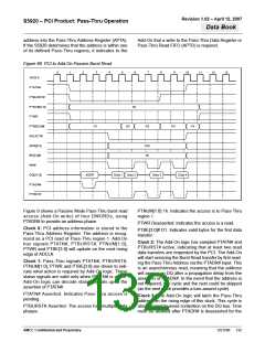
Figure 11 shows a Pass-Thru write operation for a
region defined for an 8-bit Add-On bus interface. As
the 8-bit device is connected only to DQ[7:0], the
device must access the APTD one byte at a time.
For Pass-Thru reads (Add-On APTD writes), the bytes
requested by the PCI initiator are indicated by the
PTBE[3:0]# outputs. Add-On logic uses the
PTBE[3:0]# signals to determine which bytes must be
written (and which bytes have already been written).
For example, a PCI initiator performs a byte Pass-Thru
read from an 8-bit Pass-Thru region with PCI BE2#
asserted. On the Add-On interface, PTBE2# is
asserted, indicating that the PCI initiator requires data
on this byte lane. Once the Add-On writes APTD, byte
A PCI initiator has performed a posted burst-write of
two DWORDs to Pass-Thru region zero. Data0 =
08D49A30h and Data1 = AABBCCDDh. All byte-
enables of the DWORDs were active.
Clock 0: The address is recognized as a PCI write to
Pass-Thru region 0. The PCI bus write address is
stored in the Pass-Thru Address Register. The PCI
bus write data is stored in the S5920 write FIFO. Add-
AMCC Confidential and Proprietary
DS1596
135

 AMCC [ APPLIED MICRO CIRCUITS CORPORATION ]