Revision 1.02 – April 12, 2007
S5920 – PCI Product: Pass-Thru Operation
Data Book
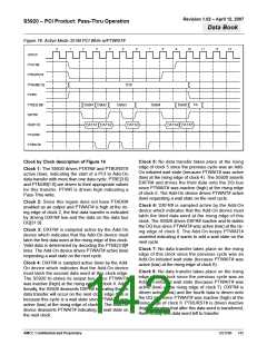
Clock 9: DXFR# is sampled active (low) by the Add-
On device which indicates that the Add-On device
must latch the fourth data word at the rising edge of
this clock. PTATN# is driven inactive (high) indicating
that this will be the last data phase.
Clock 11: PTBE# may change state.
Figure 17 shows a Pass-Thru Burst Write data transfer
in which the S5920 has been programmed to strobe
data using a one-wait state delay. The Add-On device
leaves PTWAIT# inactive (high) for all time.
Clock 10: DXFR# is sampled active (low) by the Add-
On device which indicates that the Add-On device
must latch the fifth data word at the rising edge of this
clock.
Clock by Clock description of Figure 17
Clock 1: The S5920 drives PTATN# and PTBURST#
active (low) indicating the start of a PCI to Add-On
data transfer with more than one data cycle. PTBE[3:0]
and PTNUM[1:0] are driven to their appropriate values
for this transfer. PTWR is driven high indicating a
Pass-Thru write.
DXFR# is deasserted since the access is complete.
PTBE# is driven to Fh indicating all 4 bytes have been
accessed. PTNUM and PTWR may change state
since the access is complete.
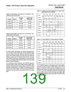
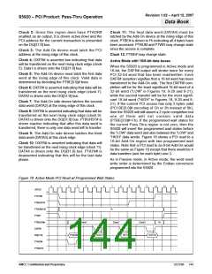
Figure 77. Active Mode PCI Write Showing a One Wait State Programmed Delay
3
4
9
0
1
2
5
6
7
8
10
11
12
13
ADCLK
PTATN#
PTBURST#
PTNUM[1:0]
PTWR
1h
PTBE[3:0]#
DXFR#
Data1
Data2
DATA2
Data3
Data4
Fh
DQ[31:0]
PTADR#
PTWAIT#
PTADDR
DATA1
DATA3
DATA4
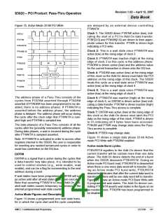
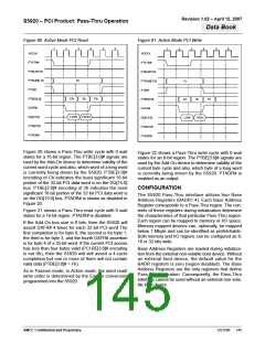
Figure 78. 16-Bit Active Mode PCI Read w/ Programmed Wait States
3
4
9
14
7
8
0
1
2
5
6
10
11
12
13
ADCLK
PTATN#
PTBURST#
PTNUM[1:0]
PTWR
1h
PTBE[3:0]#
DXFR#
Ch
3h
Fh
DQ[15:0]
PTADR#
PTWAIT#
PTADDR
LOW
HIGH
AMCC Confidential and Proprietary
DS1596
143

 AMCC [ APPLIED MICRO CIRCUITS CORPORATION ]