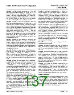
Revision 1.02 – April 12, 2007
S5920 – PCI Product: Pass-Thru Operation
Data Book
Clock 5: The Add-On logic latches BYTE1. RD# and
BE2# are sampled asserted by the S5920, so BYTE2
of the APTD is driven on DQ[7:0] and PTBE2# is deas-
serted. The Add-On device asserts RD# and BE3#,
thus requesting that BYTE3 of the APTD be driven on
the DQ bus during the next cycle. PTRDY# is also
asserted, indicating that the transfer is complete.
Clock 11: The Add-On logic latches BYTE0 of the
second DWORD. PTATN# and PTBURST# both deas-
serted indicate that the Pass-Thru transfer is
complete. The PCI can start another access on the
next clock cycle. For 16-bit peripheral devices, the
byte steering works in the same way. Because the
Add-On data bus is 16 bits wide, only two 16-bit cycles
are required to access the entire APTD Register. Two
byte enables can be asserted during each access.
Clock 6: The Add-On logic latches BYTE2. RD# and
BE3# are sampled asserted by the S5920, so BYTE3
of the APTD is driven on DQ[7:0]. PTRDY# is sampled
asserted, so the previous transfer is complete. The
PTBE# signals are updated to indicate which bytes are
valid for the next transfer (in this case, all bytes are
valid for the second DWORD, so PTBE# = 0h). The
S5920 deasserts PTBURST#, as it only has one
DWORD left to transfer. The Add-On device asserts
RD# and BE3#, thus requesting that BYTE3 of the
second DWORD in the APTD be driven on the DQ bus
during the next cycle.
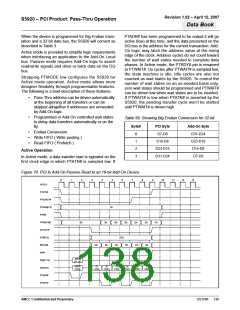
Figure 12 shows a Pass-Thru read operation for a
region defined for a 16-bit Add-On bus interface. As
the 16-bit device is connected only to DQ[15:0], the
device must access the APTD one word at a time. The
Add-On must be capable of latching the upper 16 bits
of the APTA (if they are needed).
The PCI initiator has requested a 32-bit burst read
from Pass-Thru region three. All PTBE#s are asserted.
Clock 1: The Add-On begins by reading the APTA
register (asserting PTADR#). All 32 bits of the address
are driven on the DQ bus.
Clock 7: The Add-On logic latches BYTE3 of the first
DWORD. RD# and BE3# are sampled asserted by the
S5920, so BYTE3 of the second DWORD in the APTD
is driven on DQ[7:0] and PTBE3# is deasserted. The
Add-On device asserts RD# and BE2#, thus request-
ing that BYTE2 of the APTD be driven on the DQ bus
during the next cycle.
Clock 2: Turn-around cycle, preventing potential bus
contention on the DQ bus.
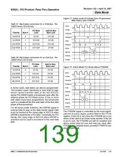
Clock 3: The Add-On initiates the write by asserting
WR#, SELECT#, BE[3:0]# = “1100”, ADR[6:2] = 2Ch
and the low word of the first DWORD to be transferred
(D0-LO).
Clock 8: The Add-On logic latches BYTE3 of the sec-
ond DWORD. RD# and BE2# are sampled asserted
by the S5920, so BYTE2 of the APTD is driven on
DQ[7:0] and PTBE2# is deasserted. The Add-On
asserts RD# and BE1#, thus requesting that BYTE1 of
the APTD be driven on the DQ bus during the next
cycle.
Clock 4: The S5920 updates the PTBE#s to indicate
that the low word was provided, and that the upper
word is still required. The Add-On drives the upper
word (D0-HI), and activates the appropriate byte
enables, BE# = 0011 The Add-On also asserts
PTRDY#, indicating that it is done with the current
DWORD, and to advance the FIFO pointer and pre-
pare for the second DWORD.
Clock 9: The Add-On logic latches BYTE2 of the sec-
ond DWORD. RD# and BE1# are sampled by the
S5920, so BYTE1 of the APTD is driven on DQ[7:0]
and PTBE1# is deasserted. The Add-On asserts RD#
and BE0#, thus requesting that BYTE0 of the APTD be
driven on the DQ bus during the next cycle. PTRDY#
is also asserted, indicating that the transfer is com-
plete. As PTBURST# is already deasserted, the Add-
On recognizes that this is the last transfer.
Clock 5: The PTBE#s are updated to indicate that the
next DWORD to be transferred requires all bytes. The
Add-On drives DQ[15:0] with the lower word of the
second DWORD (D1-LO), and the byte-enables indi-
cate the same, BE# = 1100. The Add-On also
deasserts PTRDY#. This process continues until the
transfer is complete and all words have been written.
Clock 10: The Add-On logic latches BYTE1 of the
second DWORD. RD# and BE0# are sampled by the
S5920, so BYTE0 of the APTD is driven on DQ[7:0].
PTRDY# is sampled asserted, so the previous transfer
is complete. The PTBE# signals are updated to indi-
cate which bytes are valid for the next transfer (in this
case, there is no more valid data to transfer, so PTBE
= Fh). The S5920 deasserts PTATN#, as it has no data
left to transfer. The Add-On device deasserts RD#,
BE#, ADR[6:2], SELECT# as the data transfer is
complete.
Endian Conversion
Endian conversion can be enabled/disabled for each
Pass-Thru Region. It is controlled by bits 6, 14, 22 and
30 of the PTCR. The default endian type for the S5920
is Little Endian. For this reason, the default values in
the PTCR are for Little Endian. If Big Endian is
selected, the Pass-Thru data and byte-enable inter-
face will be converted to Big Endian type.
AMCC Confidential and Proprietary
DS1596
137

 AMCC [ APPLIED MICRO CIRCUITS CORPORATION ]