Revision 1.02 – April 12, 2007
S5920 – PCI Product: Pass-Thru Operation
Data Book
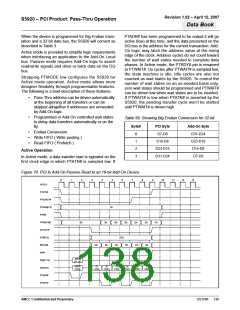
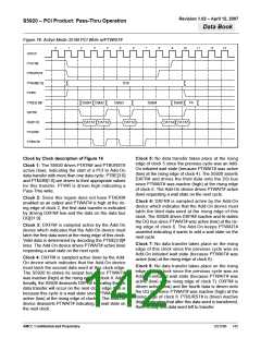
Figure 75. Active Mode 32-Bit PCI Write
are delayed by an external device controlling
PTWAIT#.
1
2
3
4
5
6
Clock 1: The S5920 drives PTATN# active (low), indi-
cating the start of a PCI to Add-On data transfer.
PTBE[3:0] and PTNUM[1:0] are driven to their appro-
priate values for this transfer. PTWR is driven high
indicating a PCI write.
ADCLK
PTATN#
PTBURST#
PTNUM[1:0]
PTWR
Clock 2: This is a wait state since PTWAIT# was
active (low) at the rising edge of clock 2.
01b
0h
Clock 3: PTWAIT# was inactive (high) at the rising
edge of clock 3 so this cycle is the address phase:
PTADR# is driven active (low) and the address value
for the current transaction is driven onto the DQ bus.
PTBE[3:0]
DXFR#
Fh
Clock 4: PTADR# was active (low) at the rising edge
of this clock so the Add-On device must latch the PCI
address on the rising edge of this clock. The S5920
treats this cycle as a wait state since PTWAIT# was
active (low) at the rising edge of clock 4.
PTADDR
DQ[31:0]
PTWAIT#
PTADR#
DATA
Clock 5: This is a wait state since PTWAIT# was
active (low) at the rising edge of clock 5.
The address phase of a Pass-Thru consists of the
cycles from PTATN# asserted through PTADR#
asserted (if PTADR# has been programmed to be dis-
abled, there is no address phase). If PTWAIT# is
asserted before the address phase, the address
phase is delayed. The address phase will occur during
the cycle after the clock edge that PTWAIT# is sam-
pled high and PTATN# is sampled low.
Clock 6: PTWAIT# was inactive (high) at the rising
edge of clock 6, so DXFR# is driven active (low) indi-
cating a data transfer. PTATN# is driven inactive (high)
indicating the Pass-Thru access is complete.
Clock 7: DXFR# was active (low) at the rising edge of
this clock so the Add-On device must latch the PCI
data on the rising edge of this clock. PTBE# is driven
to Fh indicating all 4 bytes have been accessed.
PTNUM and PTWR may change state since the Pass-
Thru access is complete.
The data phase(s) of a Pass-Thru consists of all the
cycles after the (possibly nonexistent) address phase.
During data phases, a wait is incurred during the cycle
after PTWAIT# is sampled asserted.
Clock 8: PTBE# may change state.
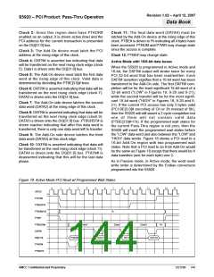
Figure 15 shows a single data phase 32-bit Active
mode PCI Write with PTADR# enabled.
Note: If PTWAIT# is activated in order to access other
registers internal to the S5920, the user is responsible
for inserting any needed turnaround cycles in order to
avoid bus contention on the DQ bus.
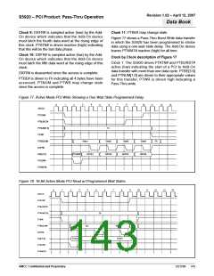
Active mode Burst cycles
PTBURST# signifies to the Add-On device that the
current transfer will be contain more than one data
phase. The Add-On device detects the end of a burst
when the S5920 deasserts PTBURST#. During an
Active mode PCI burst read, PTBURST# is deasserted
when there is one more data word left to transfer. Dur-
ing an Active mode PCI burst write, PTBURST#
deasserted indicates that after the current data word is
transferred, there will be one data word left to transfer.
Figure 16 shows an Active mode PCI Burst Write with
0 programmed wait states. The Add-On device con-
trolling PTWAIT# asserts wait states in the figure on an
as-needed basis. PTADR# has been programmed to
be disabled.
DXFR#
DXFR# is a signal that is active during the cycles that
a data transfer may take place. It is intended to be
used to control strobes (e.g., write enable, read
enable), and can be a flag for incrementing to the next
address during a burst.
If wait states have been programmed, DXFR# will not
go active until after all wait states have been executed.
Note that asserting PTWAIT# to insert Add-On initi-
ated wait states causes temporary suspension of the
internal programmed wait state counter.
Active Mode Figures and Descriptions
Figure 14 shows a programmed zero wait state trans-
fer in which the cycle start and the cycle completion
AMCC Confidential and Proprietary
DS1596
141

 AMCC [ APPLIED MICRO CIRCUITS CORPORATION ]