S2066
QUAD GIGABIT ETHERNET TRANSCEIVER
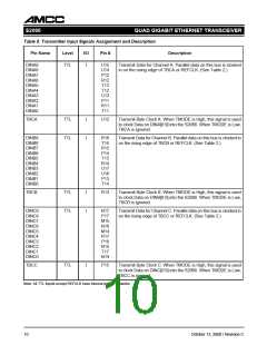
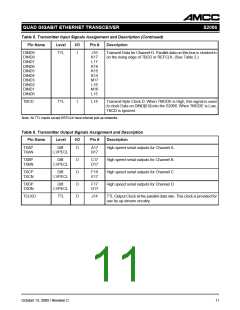
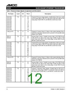
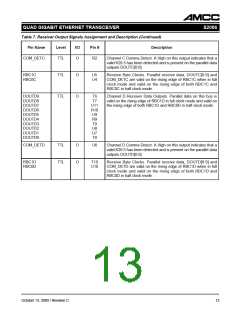
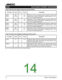
Table 8. Receiver Input Signals Assignment and Description
Pin Name
Level
I/O
Pin #
Description
RXAP
RXAN
Diff.
LVPECL
I
D4
B3
Differential LVPECL compatible inputs for channel A. RXAP is the
positive input, RXAN is the negative. Internally biased to VDD-
1.3V for AC coupled applications.
RXBP
RXBN
Diff.
LVPECL
I
I
I
C6
B5
Differential LVPECL compatible inputs for channel B. RXBP is the
positive input, RXBN is the negative. Internally biased to VDD-
1.3V for AC coupled applications.
RXCP
RXCN
Diff.
LVPECL
A8
A9
Differential LVPECL compatible inputs for channel C. RXCP is the
positive input, RXCN is the negative. Internally biased to VDD-
1.3V for AC coupled applications.
RXDP
RXDN
Diff.
LVPECL
C11
B12
Differential LVPECL compatible inputs for channel D. RXDP is the
positive input, RXDN is the negative. Internally biased to VDD-
1.3V for AC coupled applications.
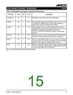
Table 9. Receiver Control Signals Assignment and Description
Pin Name
LPEN
Level
I/O
Pin #
Description
TTL
I
D14
Loopback Enable. When Low, input source for each channel is the
high speed serial output. When High, the serial output for each
channel is looped back to its input.
CMODE
TTL
I
C2
Clock Mode Control. When Low, the parallel output clocks
(RBC1/0x) rate equals 1/2 the data rate. When High, the parallel
output clocks (RBC1/0x) rate is equal to the data rate.
Note: All TTL inputs except REFCLK have internal pull-up networks.
14
October 13, 2000 / Revision C

 AMCC [ APPLIED MICRO CIRCUITS CORPORATION ]