S2066
QUAD GIGABIT ETHERNET TRANSCEIVER
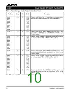
Table 7. Receiver Output Signals Assignment and Description
Pin Name
Level
I/O
Pin #
Description
DOUTA9
TTL
O
G1
G3
J1
J3
J2
H1
H2
H3
F1
G2
Channel A Receiver Data Outputs. Parallel data on this bus is valid
on the rising edge of RBC1A in full clock mode and valid on the
rising edge of both RBC1A and RBC0A in half clock mode.
DOUTA8
DOUTA7
DOUTA6
DOUTA5
DOUTA4
DOUTA3
DOUTA2
DOUTA1
DOUTA0
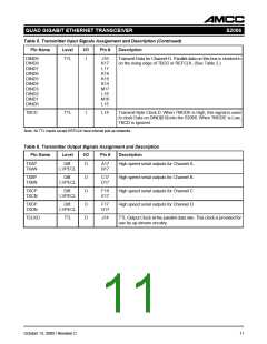
COM_DETA
TTL
TTL
O
O
F2
Channel A Comma Detect. A High on this output indicates that a
valid K28.5 has been detected and is present on the parallel data
outputs DOUTA[0:9].
RBC1A
RBC0A
K2
K1
Receive Byte Clocks. Parallel receive data, DOUTA[0:9] and
COM_DETA are valid on the rising edge of RBC1A when in full
clock mode and valid on the rising edge of both RBC1A and
RBC0A in half clock mode.
DOUTB9
DOUTB8
DOUTB7
DOUTB6
DOUTB5
DOUTB4
DOUTB3
DOUTB2
DOUTB1
DOUTB0
TTL
O
K3
P2
R1
P1
M3
N2
M2
N1
L2
Channel B Receiver Data Outputs. Parallel data on this bus is valid
on the rising edge of RBC1B in full clock mode and valid on the
rising edge of both RBC1B and RBC0B in half clock mode.
M1
COM_DETB
TTL
TTL
O
O
L1
Channel B Comma Detect. A High on this output indicates that a
valid K28.5 has been detected and is present on the parallel data
outputs DOUTB[0:9].
RBC1B
RBC0B
U1
T1
Receive Byte Clocks. Parallel receive data, DOUTB[0:9] and
COM_DETB are valid on the rising edge of RBC1B when in full
clock mode and valid on the rising edge of both RBC1B and
RBC0B in half clock mode.
DOUTC9
DOUTC8
DOUTC7
DOUTC6
DOUTC5
DOUTC4
DOUTC3
DOUTC2
DOUTC1
DOUTC0
TTL
O
T2
P3
R7
R6
T5
U3
T4
R5
U2
T3
Channel C Receiver Data Outputs. Parallel data on this bus is
valid on the rising edge of RBC1C in full clock mode and valid on
the rising edge of both RBC1C and RBC0C in half clock mode.
12
October 13, 2000 / Revision C

 AMCC [ APPLIED MICRO CIRCUITS CORPORATION ]