QUAD GIGABIT ETHERNET TRANSCEIVER
S2066
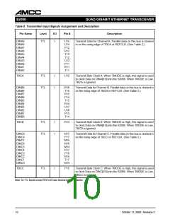
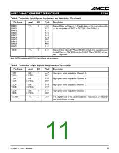
Table 5. Transmitter Input Signals Assignment and Description (Continued)
Pin Name
Level
I/O
Pin #
Description
DIND9
TTL
I
J16
K17
L17
K16
K15
K14
M17
L16
M16
L15
Transmit Data for Channel D. Parallel data on this bus is clocked in
on the rising edge of TBCD or REFCLK. (See Table 2.)
DIND8
DIND7
DIND6
DIND5
DIND4
DIND3
DIND2
DIND1
DIND0
TBCD
TTL
I
L14
Transmit Byte Clock D. When TMODE is High, this signal is used
to clock Data on DIND[0:9] into the S2066. When TMODE is Low,
TBCD is ignored.
Note: All TTL inputs except REFCLK have internal pull-up networks.
Table 6. Transmitter Output Signals Assignment and Description
Pin Name
Level
I/O
Pin #
Description
TXAP
TXAN
Diff.
LVPECL
O
A17
B17
High speed serial outputs for Channel A.
TXBP
TXBN
Diff.
LVPECL
O
O
O
O
C17
D17
High speed serial outputs for Channel B.
High speed serial outputs for Channel C.
High speed serial outputs for Channel D.
TXCP
TXCN
Diff.
LVPECL
F16
E17
TXDP
TXDN
Diff.
LVPECL
F17
G17
TCLKO
TTL
J14
TTL Output Clock at the parallel data rate. This clock is provided for
use by up-stream circuitry.
11
October 13, 2000 / Revision C

 AMCC [ APPLIED MICRO CIRCUITS CORPORATION ]