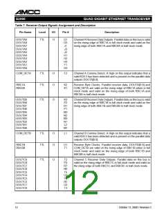
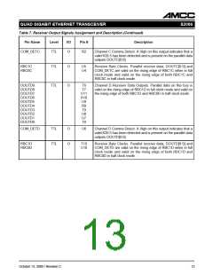
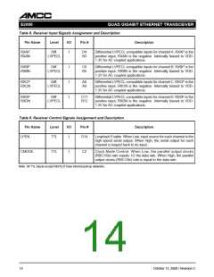
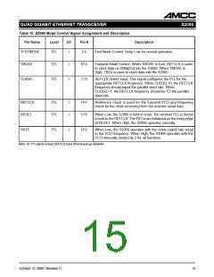
S2066
QUAD GIGABIT ETHERNET TRANSCEIVER
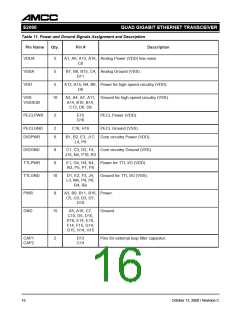
Table 11. Power and Ground Signals Assignment and Description
Pin Name
Qty.
Pin #
Description
VDDA
5
A1, A6, A13, A16, Analog Power (VDD) low noise.
C8
VSSA
VDD
5
5
B7, B8, B15, C4, Analog Ground (VSS).
D11
A12, A15, B4, B6, Power for high speed circuitry (VDD).
D9
VSS
10
A2, A4, A7, A11, Ground for high speed circuitry (VSS).
VSSSUB
A14, B10, B14,
C13, D6, D8
PECLPWR
2
E15
G16
PECL Power (VDD).
PECL Ground (VSS).
PECLGND
DIGPWR
2
6
C16, H16
B1, B2, E3, J17, Core circuitry Power (VDD).
L4, P9
DIGGND
TTLPWR
TTLGND
8
8
C1, C3, D2, F4, Core circuitry Ground (VSS).
J15, N4, P10, R3
E1, G4, H4, K4, Power for TTL I/O (VDD).
N3, P5, P7, P8
10
D1, E2, F3, J4,
L3, M4, P4, P6,
R4, R8
Ground for TTL I/O (VSS).
PWR
GND
9
A3, B9, B11, B16, Power.
C5, C9, D3, D7,
D10
15
A5, A10, C7,
C10, D5, D15,
D16, E14, E16,
F14, F15, G14,
G15, H14, H15
Ground.
CAP1
CAP2
2
D13
C14
Pins for external loop filter capacitor.
16
October 13, 2000 / Revision C

 AMCC [ APPLIED MICRO CIRCUITS CORPORATION ]