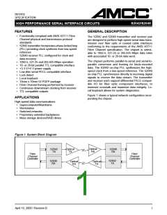
S2042/S2048
HIGH PERFORMANCE SERIAL INTERFACE CIRCUITS
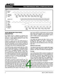
Figure 5. Functional Waveform
S
REFCLK
(Input)
2
0
PARALLEL
DATA BUS
(Input)
4
K28.5,
Byte 1
of Data
Byte 2, 3 Byte 4, 5
of Data of Data
Byte 6, 7
of Data
Byte 14,15
of Data
K28.5
Byte 16
of Data
Byte 8, 9
of Data 11 of Data 13 of Data
Byte 10, Byte 12,
2
SERIAL DATA
D2
D1
D3
D5
D4
D6
D8
D7
D9
D10 D11 D12
K28.5
D14
K28.5
D16
D13
D15
RCLK
(Output)
S
2
0
4
8
SYNC
(Output)
PARALLEL
DATA BUS
(Output)
K28.5,
Byte 1
of Data
Byte 2, 3
of Data
Byte 4, 5
of Data
Byte 6, 7
of Data
Byte 14,15
of Data
Byte 8, 9
of Data 11 of Data 13 of Data
Byte 10,
Byte 12,
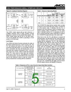
word clock (RCLK) is synchronized to the incoming
data stream word boundary by the detection of the
Fiber Channel COMMA synchronization pattern
(0011111XXX, positive running disparity).
S2048 RECEIVER FUNCTIONAL
DESCRIPTION
The S2048 receiver is designed to implement the
ANSI X3T11 Fibre Channel specification receiver
functions. A block diagram showing the basic chip
function is provided in Figure 4.
10-Bit/20-Bit Mode
The S2048 will operate with either 10-bit or 20-bit
parallel data outputs. This option is selectable via
the DWS pin. See Tables 1 and 3. In 10-bit mode,
D[10:19] are used and D[0:9] are driven to the logic
high state.
Whenever a signal is present, the S2048 attempts to
achieve synchronization on both bit and transmis-
sion-word boundaries of the received encoded bit
stream. Received data from the incoming bit stream
is provided on the device’s parallel data outputs.
Reference Clock Input
The S2048 accepts serial encoded data from a fiber
optic or coaxial cable interface. The serial input stream
is the result of the serialization of 8B/10B encoded
data by an FC compatible transmitter. Clock recov-
ery is performed on-chip, with the output data
presented to the Fibre Channel transmission layer as
10- or 20-bit parallel data. The chip is programmable
to operate at the Fibre Channel specified operating
frequencies of 1062.5, 531.25 and 265.625 Mbps.
The reference clock input must be supplied with a single-
ended AC coupled crystal clock source at ±100 PPM
tolerance. See Table 3 for reference clock frequencies.
Framing
The S2048 provides SYNC character recognition and
data word alignment of the TTL level compatible out-
put data bus. During the data realignment process
the RCLK phase will be adjusted. No glitches will
occur in the RCLK signal due to the realignment. In
systems where the SYNC detect function is undes-
ired, a LOW on the SYNCEN input disables the SYNC
function and the data will be “un-framed”.
Serial/Parallel Conversion
Serial data is received on the RX and RY pins. The
PLL clock recovery circuit will lock to the data stream
if the clock to be recovered is within ±100 PPM of the
internally generated bit rate clock. The recovered clock
is used to retime the input data stream. The data is
then clocked into the serial-to-parallel output regis-
ters. The parallel data out can be either 10- or 20-bits
wide determined by the state of the DWS pin. The
When framing is disabled by low SYNCEN, the S2048
achieves bit synchronization and begins to deliver
parallel output data words whenever it has received
full transmission words. No attempt is made to syn-
chronize on any particular incoming character.
April 10, 2000 / Revision B
4

 AMCC [ APPLIED MICRO CIRCUITS CORPORATION ]