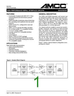
S2042/S2048
HIGH PERFORMANCE SERIAL INTERFACE CIRCUITS
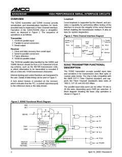
Parallel/Serial Conversion
Reference Clock Input
The parallel-to-serial converter takes in 10-bit or 20-
bit wide data from the input latch and converts it to a
serial data stream. Parallel data is latched into the
transmitter on the positive going edge of REFCLK.
The data is then clocked synchronous to the clock
synthesis unit serial clock into the serial output shift
register. The shift register is clocked by the internally
generated bit clock which is 10 times the REFCLK
input frequency. The state of the serial outputs is
controlled by the output enable pins, OE0 and OE1.
D[10] is transmitted first in 10-bit mode. D[0] is trans-
mitted first in 20-bit mode. Table 2 shows the mapping
of the parallel data to the 8B/10B codes.
The reference clock input (REFCLK) must be sup-
plied with a single-ended AC coupled crystal clock
source with ±100 PPM tolerance to assure that the
transmitted data meets the Fibre Channel frequency
limits. The internal serial clock is frequency locked to
the reference clock. The word rate clock (TCLK, TCLKN)
output frequency is determined by the selected oper-
ating speed and word width. Refer to Table 1 for
TCLK/TCLKN clock frequencies.
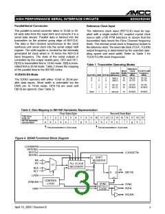
Table 1. Transmitter Operating Modes
Reference
Clock
Word
TCLK/TCLKN
Width Frequency Frequency
Data Rate
(Mbits/sec)
10-Bit/20-Bit Mode
RATESEL DWS REFSEL
(Bits)
(MHz)
(MHz)
0
0
1
0
1
0
10
20
106.25
53.125
53.125
53.125
1062.5
1062.5
The S2042 operates with either 10-bit or 20-bit par-
allel data inputs. Word width is selectable via the
DWS pin. In 10-bit mode, D[10:19] are used and
D[0:9] are ignored. (See Table 2).
1
1
1
0
1
0
10
20
53.125
26.5625
53.125
26.5625
531.25
531.25
Open
1
1
10
26.5625
26.5625
265.625
Table 2. Data Mapping to 8B/10B Alphabetic Representation
First Data Byte
Second Data Byte
TX[0:19] or
0
a
1
b
2
c
3
d
4
e
5
i
6
f
7
g
8
h
9
j
10 11 12 13 14 15 16 17 18 19
RX[0:19]
8B/10B alphabetic
representation
a
b
c
d
e
i
f
g
h
j
First bit transmitted in 20-bit mode
First bit transmitted in 10-bit mode
Figure 4. S2048 Functional Block Diagram
LOCKREFN
RATESEL
REFCLK
LOCKDETN
REFSEL
SHIFT
D
RX
REGISTER
RY
PLL CLOCK
RECOVERY
2:1
RLX
RLY
20
BITCLK
D
Q
D[0:19]
LPEN
CONTROL
SYNCEN
LOGIC
SYNC
DETECT
LOGIC
SYNC
RCLK
DWS
RCLKN
April 10, 2000 / Revision B
3

 AMCC [ APPLIED MICRO CIRCUITS CORPORATION ]