S2042/S2048
OVERVIEW
HIGH PERFORMANCE SERIAL INTERFACE CIRCUITS
Loopback
Local loopback is supported by the chipset, and pro-
vides a capability for performing offline testing of the
interface to ensure the integrity of the serial channel
before enabling the transmission medium. It also al-
lows for system diagnostics.
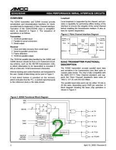
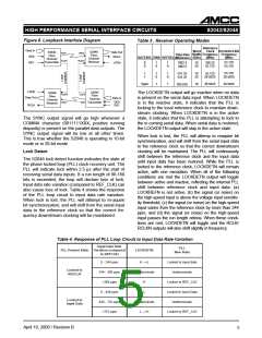
The S2042 transmitter and S2048 receiver provide
serialization and deserialization functions for block-
encoded data to implement a Fibre Channel interface.
Operation of the S2042/S2048 chips is straightfor-
ward, as depicted in Figure 2. The sequence of
operations is as follows:
Figure 2. Fibre Channel Interface Diagram
Transmitter
Parallel
Data Out
Parallel
Data In
1. 10/20-bit parallel input
2. Parallel-to-serial conversion
3. Serial output
Serial
Data
TCLK
RCLK
TX/Y
RX/Y
S2042
Transmitter
S2048
Receiver
Receiver
SYNC
Loopback
TLX/Y
1. Clock and data recovery from serial input
2. Serial-to-parallel conversion
3. Frame detection
RLX/Y
REFCLK
REFCLK
Loopback
4. 10/20-bit parallel output
LOCKDETN
The 10/20-bit parallel data handled by the S2042 and
S2048 devices should be from a DC-balanced encod-
ing scheme, such as the 8B/10B transmission code,
in which information to be transmitted is encoded 8
bits at a time into 10-bit transmission characters.
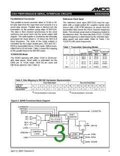
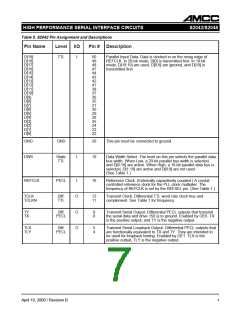
S2042 TRANSMITTER FUNCTIONAL
DESCRIPTION
The S2042 transmitter accepts parallel input data
and serializes it for transmission over fiber optic or
coaxial cable media. The chip is fully compatible with
the ANSI X3T11 Fibre Channel standard, and sup-
ports the Fibre Channel standard's data rates of
1062.5, 531.25 and 265.625 Mbps.
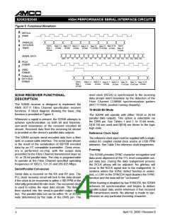
Internal clocking and control functions are transparent to
the user. Details of data timing can be seen in Figure 5.
A lock detect feature is provided on the receiver,
which indicates that the PLL is locked (synchronized)
to the reference clock or the data stream.
The parallel input data word can be either 10 bits or
20 bits wide, depending upon DWS pin selection. A
block diagram showing the basic chip operation is
shown in Figure 3.
Figure 3. S2042 Functional Block Diagram
OE0
OE1
10
10
20
2:1
D
Q
D[0:19]
10
TX
TY
DIVIDE-BY-2
SHIFT
REGISTER
TEST
DWS
TLX
TLY
CONTROL
LOGIC
TCLK
DIVIDE-BY-2
PLL CLOCK
MULTIPLIER
= F X 10/20
REFCLK
REFSEL
RATESEL
TCLKN
F
0
1
April 10, 2000 / Revision B
2

 AMCC [ APPLIED MICRO CIRCUITS CORPORATION ]