S2042/S2048
HIGH PERFORMANCE SERIAL INTERFACE CIRCUITS
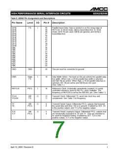
Table 5. S2042 Pin Assignment and Descriptions
Pin Name
Level I/O
Pin # Description
D[19]
D[18]
D[17]
D[16]
D[15]
D[14]
D[13]
D[12]
D[11]
D[10]
D[9]
TTL
I
50
49
48
47
44
43
42
41
38
37
36
35
31
30
29
28
25
24
23
22
Parallel Input Data. Data is clocked in on the rising edge of
REFCLK. In 20-bit mode, D[0] is transmitted first. In 10-bit
mode, D[10:19] are used, D[0:9] are ignored, and D[10] is
transmitted first.
D[8]
D[7]
D[6]
D[5]
D[4]
D[3]
D[2]
D[1]
D[0]
GND
DWS
GND
20
This pin must be connected to ground.
Static
TTL
I
19
Data Width Select. The level on this pin selects the parallel data
bus width. When Low, a 20-bit parallel bus width is selected,
and D[0:19] are active. When High, a 10-bit parallel data bus is
selected, D[1:19] are active and D[0:9] are not used.
(See Table 1.)
REFCLK
PECL
I
16
Reference Clock. (Externally capacitively coupled.) A crystal-
controlled reference clock for the PLL clock multiplier. The
frequency of REFCLK is set by the REFSEL pin. (See Table 1.)
TCLK
Diff.
TTL
O
O
O
12
11
Transmit Clock. Differential TTL word rate clock true and
complement. See Table 1 for frequency.
TCLKN
TY
TX
Diff.
PECL
9
8
Transmit Serial Output. Differential PECL outputs that transmit
the serial data and drive 150 Ω to ground. Enabled by OE0. TX
is the positive output, and TY is the negative output.
TLX
TLY
Diff.
PECL
5
4
Transmit Serial Loopback Output. Differential PECL outputs that
are functionally equivalent to TX and TY. They are intended to
be used for loopback testing. Enabled by OE1. TLX is the
positive output, TLY is the negative output.
April 10, 2000 / Revision B
7

 AMCC [ APPLIED MICRO CIRCUITS CORPORATION ]