S2042/S2048
HIGH PERFORMANCE SERIAL INTERFACE CIRCUITS
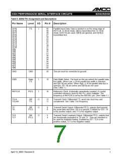
Table 6. S2048 Pin Assignment and Descriptions
Pin Name
Level I/O
Pin # Description
D[19]
D[18]
D[17]
D[16]
D[15]
D[14]
D[13]
D[12]
D[11]
D[10]
D[9]
TTL
O
45
43
42
40
38
37
35
34
32
31
29
28
25
24
22
21
18
17
15
14
Parallel data outputs. The width of the parallel data bus is
selected by the state of the DWS pin. Parallel data on this bus is
clocked out on the falling edge of RCLK in 20-bit mode and on
both the falling edges of RCLK and RCLKN in 1062.5 Mbit/sec,
10-bit mode. In 20-bit mode, D[0] is the first bit received. In 10-
bit mode, D[10:19] are used.and D[0:9] are driven to the high
state. In 10-bit mode, D[10] is the first bit received.
D[8]
D[7]
D[6]
D[5]
D[4]
D[3]
D[2]
D[1]
D[0]
LOCKDETN
TTL
TTL
O
52
Lock Detect. Active Low. When active, LOCKDETN indicates
that the PLL is locked to the incoming data stream. When
inactive, it provides a system flag indicating that the PLL is
locked to the local reference clock. This output will toggle when
no data is present on the serial data inputs.
LPEN
DWS
I
I
8
4
Loop Enable. Active High. When active, LPEN selects the
loopback differential serial input pins. When inactive, LPEN
selects RX and RY (normal operation).
Static
TTL
Data Width Select. The level on this pin selects the parallel data
bus width. When Low, a 20-bit parallel bus width is selected, and
D[0:19] are active. When High, a 10-bit parallel data bus is
selected, D[10:19] are active and D[0:9] will go HIGH. (See Table
3.) A rising edge will reset the internal counters (used for test).
RCLK
RCLKN
Diff.
TTL
O
49
48
Receive Clock. Parallel data is clocked out on the falling edge of
RCLK/RCLKN (see Timing Diagrams in Figures 13-16). After a
sync word is detected, the period of the current RCLK and
RCLKN is stretched to align with the word boundary.
(See Table 3 for frequency.)
REFCLK
SYNC
Analog
TTL
I
2
Reference Clock. (Externally capacitively coupled.) A free-
running crystal-controlled reference clock for the PLL clock
multiplier. The frequency of REFCLK is set by the REFSEL pin.
(See Table 4.)
O
51
Synchronization Detect. Upon detection of a valid sync symbol,
this output goes high for one RCLK period. When SYNC is
active, the COMMA character (0011111XXX, positive running
disparity) shall be present on the parallel data bus bits D[0:9] in
20-bit mode and D[10:19] in 10-bit mode. Gated by SYNCEN.
RLX
RLY
Diff.
PECL
I
11
12
Receive Loopback Serial Input. (Externally capacitively coupled.)
The serial loopback data inputs. RLX is the positive input, and
RLY is the negative input.
April 10, 2000 / Revision B
9

 AMCC [ APPLIED MICRO CIRCUITS CORPORATION ]