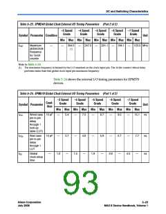
DC and Switching Characteristics
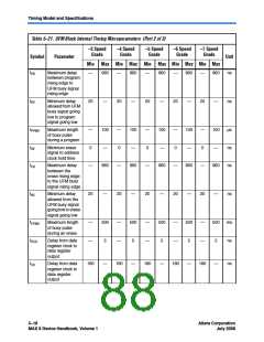
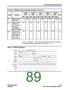
Table 5–21. UFM Block Internal Timing Microparameters (Part 3 of 3)
–3 Speed
Grade
–4 Speed
Grade
–5 Speed
Grade
–6 Speed
Grade
–7 Speed
Grade
Symbol
Parameter
Unit
Min Max Min Max Min Max Min Max Min Max
tRA
Maximum read
access time
—
65
—
65
—
65
—
65
—
65
ns
ns
tOSCS
Maximum delay
between the
250
—
250
—
250
—
250
—
250
—
OSC_ENArising
edge to the
erase/program
signal rising edge
tOSCH
Minimum delay
allowed from the
erase/program
signal going low
to OSC_ENA
250
—
250
—
250
—
250
—
250
—
ns
signal going low
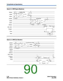
Figures 5–3 through 5–5 show the read, program, and erase waveforms
for UFM block timing parameters shown in Table 5–21.
Figure 5–3. UFM Read Waveforms
ARShft
tACLK
tAH
9 Address Bits
tASU
ARClk
tADH
ARDin
tADS
DRShft
DRClk
16 Data Bits
tDSH
tDCLK
tDSS
tDCO
DRDin
DRDout
OSC_ENA
Program
Erase
Busy
Altera Corporation
July 2008
5–19
MAX II Device Handbook, Volume 1

 ALTERA [ ALTERA CORPORATION ]