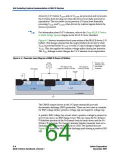
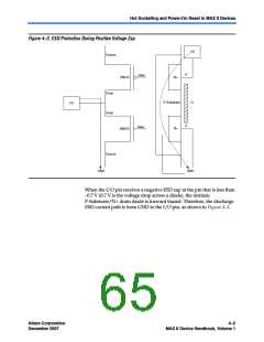
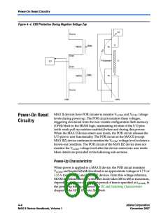
Power-On Reset Circuitry
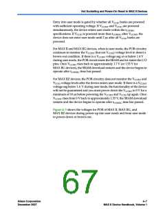
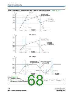
Figure 4–5. Power-Up Characteristics for MAX II, MAX IIG, and MAX IIZ Devices
Notes (1), (2)
V
3.3 V
2.5 V
MAX II Device
CCINT
Approximate Voltage
for SRAM Download Start
Device Resets
the SRAM and
Tri-States I/O Pins
1.7 V
1.4 V
t
CONFIG
0 V
User Mode
Operation
Tri-State
Tri-State
Tri-State
Tri-State
MAX IIG Device
V
CCINT
3.3 V
Approximate Voltage
for SRAM Download Start
Device Resets
the SRAM and
Tri-States I/O Pins
1.8 V
1.55 V
1.4 V
t
CONFIG
0 V
User Mode
Operation
Tri-State
MAX IIZ Device
V
CCINT
3.3 V
V
must be powered down
CCINT
to 0 V if the V
Approximate Voltage
for SRAM Download Start
CCINT
dips below this level
1.8 V
1.55 V
1.4 V
t
minimum 10 µs
t
CONFIG
CONFIG
0 V
User Mode
Operation
User Mode
Operation
Tri-State
Notes to Figure 4–5:
(1) Time scale is relative.
(2) Figure 4–5 assumes all VCCIO banks power up simultaneously with the VCCINT profile shown. If not, tCONFIG stretches
out until all VCCIO banks are powered.
4–8
Core Version a.b.c variable
Altera Corporation
December 2007
MAX II Device Handbook, Volume 1

 ALTERA [ ALTERA CORPORATION ]