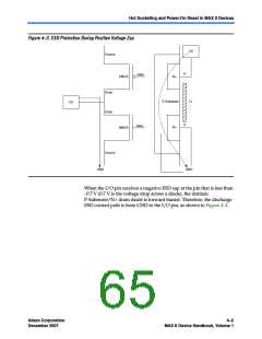
PDF
最近搜索
热门搜索
发布采购

| 型号: | EPM1270GT144I4N |
| PDF下载: | 下载PDF文件 查看货源 |
| 内容描述: | [Flash PLD, 8.1ns, 980-Cell, CMOS, PQFP144, 22 X 22 MM, 0.50 MM PITCH, LEAD FREE, TQFP-144] |
| 分类和应用: | LTE输入元件可编程逻辑 |
| 文件页数/大小: | 108 页 / 1342 K |
| 品牌: |  ALTERA [ ALTERA CORPORATION ] ALTERA [ ALTERA CORPORATION ] |
专业IC领域供求交易平台:提供全面的IC Datasheet资料和资讯,Datasheet 1000万数据,IC品牌1000多家。