Operating Conditions
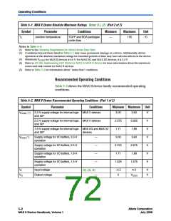
Table 5–1. MAX II Device Absolute Maximum Ratings Notes (1), (2) (Part 2 of 2)
Symbol
Parameter
Conditions
Minimum
Maximum
Unit
TJ
Junction temperature
TQFP and BGA packages
under bias
—
135
°C
Notes to Table 5–1:
(1) Refer to the Operating Requirements for Altera Devices Data Sheet.
(2) Conditions beyond those listed in Table 5–1 may cause permanent damage to a device. Additionally, device
operation at the absolute maximum ratings for extended periods of time may have adverse affects on the device.
(3) Maximum VCCINT for MAX II devices is 4.6 V. For MAX IIG and MAX IIZ devices, it is 2.4 V.
(4) Refer to AN 286: Implementing LED Drivers in MAX & MAX II Devices for more information about the maximum
source and sink current for MAX II devices.
(5) Refer to Table 5–2 for information about “under bias” conditions.
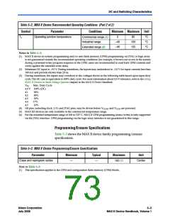
Recommended Operating Conditions
Table 5–2 shows the MAX II device family recommended operating
conditions.
Table 5–2. MAX II Device Recommended Operating Conditions (Part 1 of 2)
Symbol
Parameter
Conditions
Minimum Maximum
Unit
3.3-V supply voltage for internal logic MAX II devices
and ISP
3.00
2.375
1.71
3.60
2.625
1.89
V
VCCINT (1)
2.5-V supply voltage for internal logic MAX II devices
and ISP
V
V
V
V
V
V
1.8-V supply voltage for internal logic MAX IIG and MAX IIZ
and ISP
devices
Supply voltage for I/O buffers, 3.3-V
operation
—
—
—
—
3.00
3.60
VCCIO (1)
Supply voltage for I/O buffers, 2.5-V
operation
2.375
1.71
2.675
1.89
Supply voltage for I/O buffers, 1.8-V
operation
Supply voltage for I/O buffers, 1.5-V
operation
1.425
1.575
VI
Input voltage
–0.5
0
4.0
V
V
(2), (3), (4)
VO
Output voltage
—
VCCIO
5–2Core Version a.b.c variable
MAX II Device Handbook, Volume 1
Altera Corporation
July 2008

 ALTERA [ ALTERA CORPORATION ]