Power-On Reset Circuitry
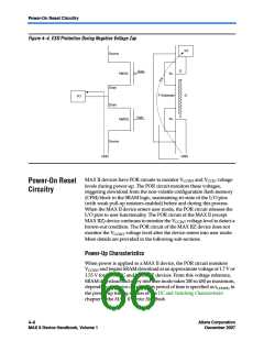
Figure 4–4. ESD Protection During Negative Voltage Zap
I/O
Source
D
Gate
PMOS
N+
Drain
P-Substrate
G
I/O
Drain
S
Gate
N+
NMOS
Source
GND
GND
MAX II devices have POR circuits to monitor VCCINT and VCCIO voltage
levels during power-up. The POR circuit monitors these voltages,
triggering download from the non-volatile configuration flash memory
(CFM) block to the SRAM logic, maintaining tri-state of the I/O pins
(with weak pull-up resistors enabled) before and during this process.
When the MAX II device enters user mode, the POR circuit releases the
I/O pins to user functionality. The POR circuit of the MAX II (except
MAX IIZ) device continues to monitor the VCCINT voltage level to detect a
brown-out condition. The POR circuit of the MAX IIZ device does not
monitor the VCCINT voltage level after the device enters into user mode.
More details are provided in the following sub-sections.
Power-On Reset
Circuitry
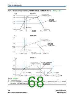
Power-Up Characteristics
When power is applied to a MAX II device, the POR circuit monitors
VCCINT and begins SRAM download at an approximate voltage of 1.7 V or
1.55 V for MAX IIG and MAX IIZ devices. From this voltage reference,
SRAM download and entry into user mode takes 200 to 450 µs maximum,
depending on device density. This period of time is specified as tCONFIG in
the power-up timing section of the DC and Switching Characteristics
chapter in the MAX II Device Handbook.
4–6
Core Version a.b.c variable
Altera Corporation
December 2007
MAX II Device Handbook, Volume 1

 ALTERA [ ALTERA CORPORATION ]