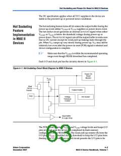
Hot Socketing Feature Implementation in MAX II Devices
driven by 3.3 V before VCCIO and/or VCCINT are powered, and it prevents
the I/O pins from driving out when the device is not fully powered or
operational. The hot socket circuit prevents I/O pins from internally
powering VCCIO and VCCINT when driven by external signals before the
device is powered.
f
For information about 5.0-V tolerance, refer to the Using MAX II Devices
in Multi-Voltage Systems chapter in the MAX II Device Handbook.
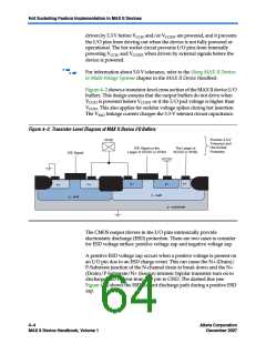
Figure 4–2 shows a transistor-level cross section of the MAX II device I/O
buffers. This design ensures that the output buffers do not drive when
VCCIO is powered before VCCINT or if the I/O pad voltage is higher than
VCCIO. This also applies for sudden voltage spikes during hot insertion.
The VPAD leakage current charges the 3.3-V tolerant circuit capacitance.
Figure 4–2. Transistor-Level Diagram of MAX II Device I/O Buffers
Ensures 3.3-V
Tolerance and
Hot-Socket
VPAD
IOE Signal or the
Larger of VCCIO or VPAD
The Larger of
VCCIO or VPAD
Protection
IOE Signal
VCCIO
p+
n+
p+
n+
n+
n -well
p -well
p -substrate
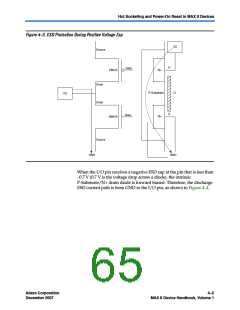
The CMOS output drivers in the I/O pins intrinsically provide
electrostatic discharge (ESD) protection. There are two cases to consider
for ESD voltage strikes: positive voltage zap and negative voltage zap.
A positive ESD voltage zap occurs when a positive voltage is present on
an I/O pin due to an ESD charge event. This can cause the N+ (Drain)/
P-Substrate junction of the N-channel drain to break down and the N+
(Drain)/P-Substrate/N+ (Source) intrinsic bipolar transistor turn on to
discharge ESD current from I/O pin to GND. The dashed line (see
Figure 4–3) shows the ESD current discharge path during a positive ESD
zap.
4–4
MAX II Device Handbook, Volume 1
Core Version a.b.c variable
Altera Corporation
December 2007

 ALTERA [ ALTERA CORPORATION ]