Arria GX Architecture
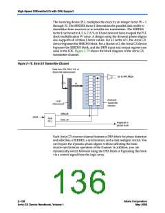
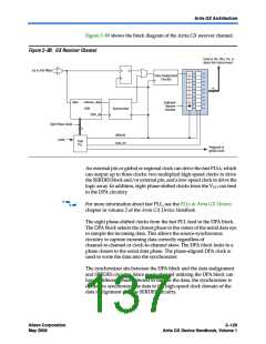
Figure 2–80 shows the block diagram of the Arria GX receiver channel.
Figure 2–80. GX Receiver Channel
Data to R4, R24, C4, or
direct link interconnect
+
–
Up to 840 Mbps
D
Q
Data Realignment
Circuitry
10
data
retimed_data
Dedicated
Receiver
Interface
DPA
Synchronizer
DPA_clk
Eight Phase Clocks
8
diffioclk
load_en
refclk
Fast
PLL
Regional or
global clock
An external pin or global or regional clock can drive the fast PLLs, which
can output up to three clocks: two multiplied high-speed clocks to drive
the SERDES block and/or external pin, and a low-speed clock to drive the
logic array. In addition, eight phase-shifted clocks from the VCO can feed
to the DPA circuitry.
f
For more information about fast PLL, see the PLLs in Arria GX Devices
chapter in volume 2 of the Arria GX Device Handbook.
The eight phase-shifted clocks from the fast PLL feed to the DPA block.
The DPA block selects the closest phase to the center of the serial data eye
to sample the incoming data. This allows the source-synchronous
circuitry to capture incoming data correctly regardless of
channel-to-channel or clock-to-channel skew. The DPA block locks to a
phase closest to the serial data phase. The phase-aligned DPA clock is
used to write the data into the synchronizer.
The synchronizer sits between the DPA block and the data realignment
and SERDES circuitry. Since every channel utilizing the DPA block can
have a different phase selected to sample the data, the synchronizer is
needed to synchronize the data to the high-speed clock domain of the
data realignment and the SERDES circuitry.
Altera Corporation
May 2008
2–129
Arria GX Device Handbook, Volume 1

 ALTERA [ ALTERA CORPORATION ]