3. Configuration and Testing
AGX51003-1.3
All ArriaTM GX devices provide Joint Test Action Group (JTAG)
boundary-scan test (BST) circuitry that complies with the IEEE Std.
1149.1. You can perform JTAG boundary-scan testing either before or
after, but not during configuration. Arria GX devices can also use the
JTAG port for configuration with the Quartus® II software or hardware
using either jam files (.jam) or jam byte-code files (.jbc).
Introduction
This chapter contains the following sections:
■
■
■
■
■
“IEEE Std. 1149.1 JTAG Boundary-Scan Support” on page 3–1
“SignalTap II Embedded Logic Analyzer” on page 3–4
“Configuration” on page 3–4
“Temperature Sensing Diode” on page 3–10
“Automated Single Event Upset (SEU) Detection” on page 3–12
Arria GX devices support I/O element (IOE) standard setting
reconfiguration through the JTAG BST chain. The JTAG chain can update
the I/O standard for all input and output pins any time before or during
user-mode through the CONFIG_IOinstruction. You can use this
capability for JTAG testing before configuration when some of the
Arria GX pins drive or receive from other devices on the board using
voltage-referenced standards. Because the Arria GX device may not be
configured before JTAG testing, the I/O pins may not be configured for
appropriate electrical standards for chip-to-chip communication.
Programming these I/O standards via JTAG allows you to fully test the
I/O connections to other devices.
IEEE Std. 1149.1
JTAG Boundary-
Scan Support
A device operating in JTAG mode uses four required pins, TDI, TDO, TMS,
and TCK, and one optional pin, TRST. The TCKpin has an internal weak
pull-down resistor, while the TDI, TMS, and TRSTpins have weak
internal pull-up resistors. The JTAG input pins are powered by the 3.3-V
VCCPDpins. The TDOoutput pin is powered by the VCCIOpower supply in
I/O bank 4.
Arria GX devices also use the JTAG port to monitor the logic operation of
the device with the SignalTap® II embedded logic analyzer. Arria GX
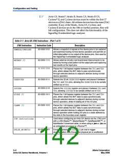
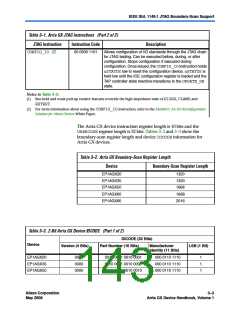
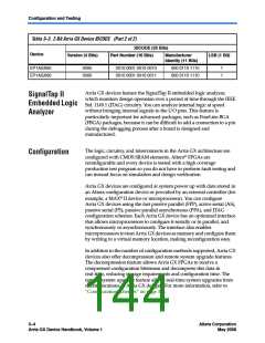
devices support the JTAG instructions shown in Table 3–1.
Altera Corporation
May 2008
3–1

 ALTERA [ ALTERA CORPORATION ]