I/O Structure
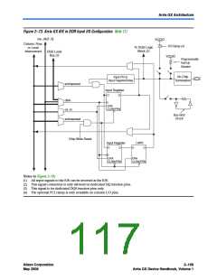
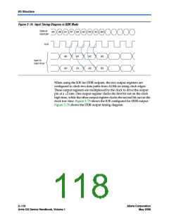
Figure 2–74. Input Timing Diagram in DDR Mode
Data at
input pin
B0
A0 B1 A1 B2 A2 B3 A3 B4
CLK
A0
B0
A1
B1
A2
B2
A3
B3
Input To
Logic Array
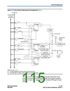
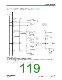
When using the IOE for DDR outputs, the two output registers are
configured to clock two data paths from ALMs on rising clock edges.
These output registers are multiplexed by the clock to drive the output
pin at a ×2 rate. One output register clocks the first bit out on the clock
high time, while the other output register clocks the second bit out on the
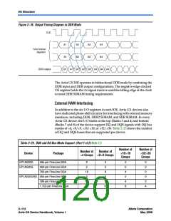
clock low time. Figure 2–75 shows the IOE configured for DDR output.
Figure 2–76 shows the DDR output timing diagram.
2–110
Arria GX Device Handbook, Volume 1
Altera Corporation
May 2008

 ALTERA [ ALTERA CORPORATION ]