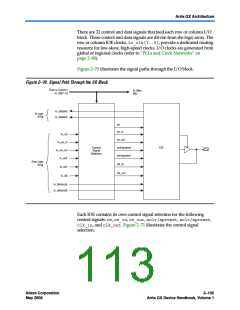
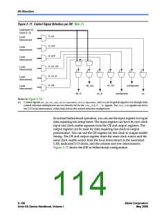
Arria GX Architecture
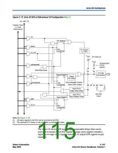
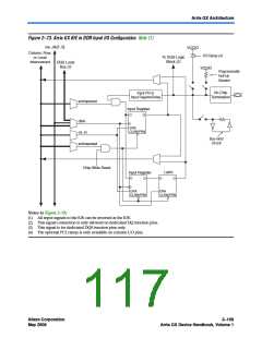
Figure 2–73. Arria GX IOE in DDR Input I/O Configuration Note (1)
ioe_clk[7..0]
VCCIO
Column, Row,
or Local
Interconnect
PCI Clamp (4)
To DQS Logic
Block (3)
DQS Local
Bus (2)
VCCIO
Programmable
Pull-Up
Resistor
On-Chip
Termination
Input Pin to
Input RegisterDelay
sclr/spreset
Input Register
D
Q
clkin
ENA
CLRN/PRN
ce_in
Bus-Hold
Circuit
aclr/apreset
Chip-Wide Reset
Latch
D Q
Input Register
D
Q
ENA
ENA
CLRN/PRN
CLRN/PRN
Notes to Figure 2–73:
(1) All input signals to the IOE can be inverted at the IOE.
(2) This signal connection is only allowed on dedicated DQ function pins.
(3) This signal is for dedicated DQS function pins only.
(4) The optional PCI clamp is only available on column I/O pins.
Altera Corporation
May 2008
2–109
Arria GX Device Handbook, Volume 1

 ALTERA [ ALTERA CORPORATION ]