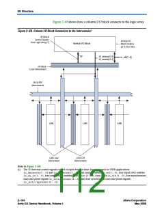
I/O Structure
A path in which a pin directly drives a register can require the delay to
ensure zero hold time, whereas a path in which a pin drives a register
through combinational logic may not require the delay. Programmable
delays exist for decreasing input-pin-to-logic-array and IOE input
register delays. The Quartus II Compiler can program these delays to
automatically minimize setup time while providing a zero hold time.
Programmable delays can increase the register-to-pin delays for output
and/or output enable registers. Programmable delays are no longer
required to ensure zero hold times for logic array register-to-IOE register
transfers. The Quartus II Compiler can create zero hold time for these
transfers. Table 2–22 shows the programmable delays for Arria GX
devices.
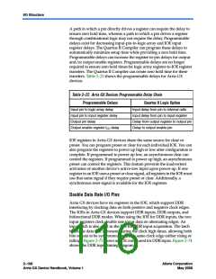
Table 2–22. Arria GX Devices Programmable Delay Chain
Programmable Delays
Quartus II Logic Option
Input pin to logic array delay
Input pin to input register delay
Output pin delay
Input delay from pin to internal cells
Input delay from pin to input register
Delay from output register to output pin
Delay to output enable pin
Output enable register tCO delay
IOE registers in Arria GX devices share the same source for clear or
preset. You can program preset or clear for each individual IOE. You can
also program the registers to power up high or low after configuration is
complete. If programmed to power up low, an asynchronous clear can
control the registers. If programmed to power up high, an asynchronous
preset can control the registers. This feature prevents the inadvertent
activation of another device’s active-low input upon power-up. If one
register in an IOE uses a preset or clear signal, all registers in the IOE must
use that same signal if they require preset or clear. Additionally, a
synchronous reset signal is available for the IOE registers.
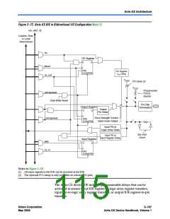
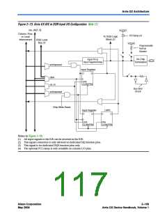
Double Data Rate I/O Pins
Arria GX devices have six registers in the IOE, which support DDR
interfacing by clocking data on both positive and negative clock edges.
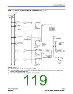
The IOEs in Arria GX devices support DDR inputs, DDR outputs, and
bidirectional DDR modes. When using the IOE for DDR inputs, the two
input registers clock double rate input data on alternating edges. An
input latch is also used in the IOE for DDR input acquisition. The latch
holds the data that is present during the clock high times, allowing both
bits of data to be synchronous with the same clock edge (either rising or
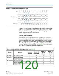
falling). Figure 2–73 shows an IOE configured for DDR input. Figure 2–74
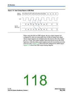
shows the DDR input timing diagram.
2–108
Arria GX Device Handbook, Volume 1
Altera Corporation
May 2008

 ALTERA [ ALTERA CORPORATION ]