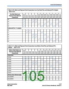
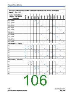
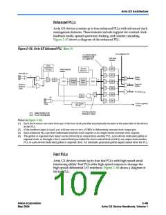
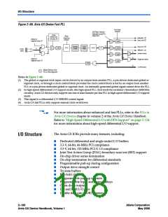
Arria GX Architecture
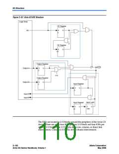
The IOE in Arria GX devices contains a bidirectional I/O buffer, six
registers, and a latch for a complete embedded bidirectional single data
rate or DDR transfer. Figure 2–67 shows the Arria GX IOE structure. The
IOE contains two input registers (plus a latch), two output registers, and
two output enable registers. The design can use both input registers and
the latch to capture DDR input and both output registers to drive DDR
outputs. Additionally, the design can use the output enable (OE) register
for fast clock-to-output enable timing. The negative edge-clocked OE
register is used for DDR SDRAM interfacing. The Quartus II software
automatically duplicates a single OE register that controls multiple
output or bidirectional pins.
Altera Corporation
May 2008
2–101
Arria GX Device Handbook, Volume 1

 ALTERA [ ALTERA CORPORATION ]