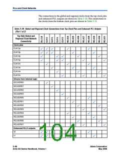
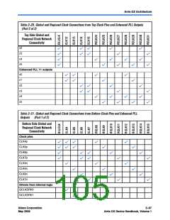
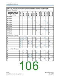
Arria GX Architecture
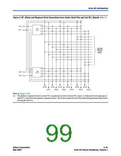
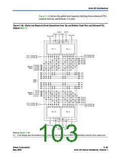
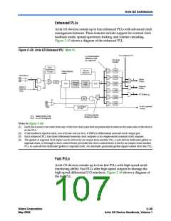
Figure 2–64 shows the global and regional clocking from enhanced PLL
outputs and top and bottom CLKpins.
Figure 2–64. Global and Regional Clock Connections from Top and Bottom Clock Pins and Enhanced PLL
Outputs Note (1)
CLK15
CLK14
CLK13
CLK12
PLL5_FB
PLL11_FB
PLL 11
PLL 5
c0 c1 c2 c3 c4 c5 c0 c1 c2 c3 c4 c5
PLL5_OUT[2..0]p
PLL5_OUT[2..0]n
PLL11_OUT[2..0]p
PLL11_OUT[2..0]n
RCLK31
RCLK30
RCLK29
RCLK28
RCLK27
Regional
Clocks
RCLK26
RCLK25
RCLK24
G15
G14
G13
G12
Global
Clocks
G4
G5
G6
G7
RCLK8
RCLK9
RCLK10
RCLK11
Regional
Clocks
RCLK12
RCLK13
RCLK14
RCLK15
PLL12_OUT[2..0]p
PLL12_OUT[2..0]n
PLL6_OUT[2..0]p
PLL6_OUT[2..0]n
c0 c1 c2 c3 c4 c5 c0 c1 c2 c3 c4 c5
PLL 12
PLL 6
PLL12_FB
PLL6_FB
CLK4
CLK6
CLK5
CLK7
Note to Figure 2–64:
(1) If the design uses the feedback input, you will lose one (or two if FBIN is differential) external clock output pin.
Altera Corporation
May 2008
2–95
Arria GX Device Handbook, Volume 1

 ALTERA [ ALTERA CORPORATION ]