PIN DESCRIPTION
Pin No.
Symbol
Description
-
1
I
Bias circuit pin. Connect a 0.1µF capacitor from this pin to V to minimize noise.
B
2
C
INT
Integrator capacitor connection.
-
V
3
Negative power supply.
4
C
The Auto-zero capacitor connection.
The Integrator resistor buffer connection.
This pin is analog ground.
AZ
5
BUF
6
AGND
-
7
C
Negative reference capacitor connection.
Positive reference capacitor connection.
REF
+
C
8
REF
-
Internally connected. Connect to V for normal operation.
9
N/C
N/C
-
10
11
12
13
14
15
16
17
Internally connected. Connect to V for normal operation.
-
V
External voltage reference (-) connection. High impedance load (≥100MΩ) only.
External voltage reference (+) connection. High impedance load (≥100MΩ) only.
Negative analog input.
REF
+
V
REF
-
V
IN
+
V
Positive analog input.
IN
A
B
C
Converter phase control MSB Input.
Converter phase control LSB Input.
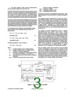
Comparator output. C
OUT
is LOW when a negative input voltage is being integrated. A HIGH-to-LOW transition on C
that the Deintegrate phase is completed. C
time the Integrator Zero phase.
is HIGH during the Integration phase when a positive input voltage is being integrated and
signals the processor
is undefined during the Auto-Zero phase. It should be monitored to
OUT
OUT
OUT
18
19
20
DGND
Digital ground.
+
V
Positive power supply.
C
S
Chip select - power down pin. Logic 1 = power on. Logic 0 = power down.
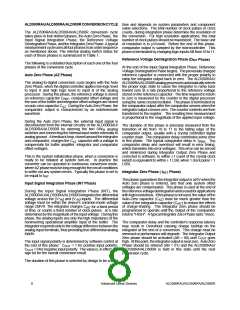
Table 1. Conversion Phase and Control Logic Internal Analog Switch Functions
Switch Functions
Input
Connect
Reference Input Auto Zero
Polarity
Reference
Sample
V
=AGND
IN
System
Offset
Conversion Control
Phase
Logic
+
-
SW
R
SW
SW
SW
SW
SW
SW
S
IN
R or
AZ
R
G
Auto Zero
A = 0, B = 1
A = 1, B = 0
Open
Open
Open
Closed
Open
Closed
Open
Closed
Open
Open
Open
Input Signal
Integration
Closed
Reference Voltage A = 1, B = 1
Deintegration
Open
Open
Closed*
Open
Open
Open
Open
Closed
Closed
Open
Integrator
A = 0, B = 0
Closed
Closed
Output Zero
+
-
R
*SW would be closed for a positive input signal. SW would be closed for a negative input signal.
R
ALD500RAU/ALD500RA/ALD500R
Advanced Linear Devices
7

 ALD [ ADVANCED LINEAR DEVICES ]