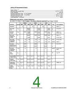
+
-
Differential Inputs (V IN,V IN)
(+) or (-) input voltages will cause a roll-over error. This error
can be minimized by using a large reference capacitor in
The ALD500RAU/ALD500RA/ALD500R operates with comparison to the stray capacitance.
differential voltages within the input amplifier common-mode
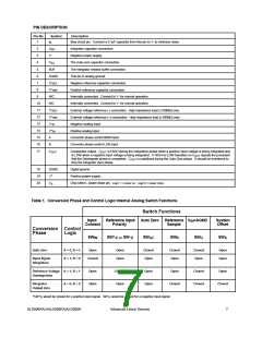
voltage range. The amplifier common-mode range extends Phase Control Inputs (A, B)
from 1.5V below positive supply to 1.5V above negative
supply. Within this common-mode voltage range, common- The A and B logic inputs select the ALD500RAU/ALD500RA/
mode rejection is typically 95dB.
ALD500R operating phase. The A and B inputs are normally
driven by a microprocessor I/O port or external logic, using
The integrator output also follows the common-mode voltage. CMOS logic levels. For logic control functions of A and B logic
When large common-mode voltages with near full-scale inputs, see Table 1.
differential input voltages are applied, the input signal drives
the integrator output to near the supply rails where the Comparator Output (COUT
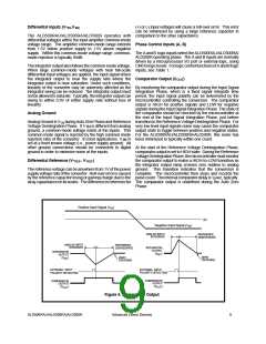
)
integrator output is near saturation. Under such conditions,
linearity of the converter may be adversely affected as the By monitoring the comparator output during the Input Signal
integrator swing can be reduced. The integrator output must Integration Phase, which is a fixed signal integrate time
notbeallowedtosaturate. Typically, theintegratoroutputcan period, the input signal polarity can be determined by the
swing to within 0.9V of either supply rails without loss of microcontroller controlling the conversion. The comparator
linearity.
output is HIGH for positive signals and LOW for negative
signals during the Input Signal Integration Phase. The state of
the comparator should be checked by the microcontroller at
the end of the Input Signal Integration Phase, just before
Analog Ground
AnalogGroundisV-IN duringAutoZeroPhaseandReference transition to the Reference Voltage Deintegration Phase. For
Voltage Deintegration Phase. If V- is different from analog very low level input signals noise may cause the comparator
ground, a common-mode voltage exists at the inputs. This output state to toggle between positive and negative states.
common mode signal is rejected by the high common mode For the ALD500RAU/ALD500RA/ALD500R, this noise has
rejection ratio of the converter. In most applications, V
set at a fixed known voltage (i.e., power supply ground). All
other ground connections should be connected to digital At the start of the Reference Voltage Deintegration Phase,
IN
-
is been minimized to typically within one count.
IN
ground in order to minimize noise at the inputs.
comparator output is set to HIGH state. During the Reference
VoltageDeintegrationPhase,themicrocontrollermustmonitor
the comparator output to make a HIGH-to-LOW transition as
the integrator output ramp crosses zero relative to analog
+
-
Differential Reference (V REF, V REF
)
The reference voltage can be anywhere from 1V of the power ground. This transition indicates that the conversion is
supply voltage rails of the converter. Roll-over error is caused complete. The microcontroller then stops and records the
by the reference capacitor losing or gaining charge due to the pulsecount. Theinternalcomparatordelayis1µsec,typically.
straycapacitanceonitsnodes. Thedifferenceinreferencefor The comparator output is undefined during the Auto Zero
Phase.
Positive Input Signal (VIN
)
0V
Negative Input Signal (VIN
)
ANALOG INPUT
REFERENCE
DEINTEGRATE
INTEGRATE
ANALOG INPUT
INTEGRATE
REFERENCE
DEINTEGRATE
INTEGRATOR
OUTPUT
INTEGRATOR
OUTPUT
(V
)
INT
ZERO
CROSSING
ZERO
CROSSING
(V
)
INT
EXTERNAL INPUT
EXTERNAL INPUT
POLARITY DETECTION
POLARITY DETECTION
COMPARATOR
OUTPUT
COMPARATOR
OUTPUT
(C
)
(C
)
OUT
OUT
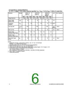
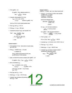
Figure 4. Comparator Output
ALD500RAU/ALD500RA/ALD500R
Advanced Linear Devices
9

 ALD [ ADVANCED LINEAR DEVICES ]