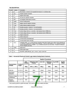
ALD500RAU/ALD500RA/ALD500RCONVERSIONCYCLE
time and depends on system parameters and component
value selections. The total number of clock pulses or clock
The ALD500RAU/ALD500RA/ALD500R conversion cycle counts, during integration phase determine the resolution of
takes place in four distinct phases, the Auto Zero Phase, the the conversion. For high resolution applications, this total
Input Signal Integration Phase, the Reference Voltage number of clock pulses should be maximized. The basic unit
Deintegration Phase, and the Integrator Zero Phase. A typical
of resolution is in µV/count. Before the end of this phase,
measurementcycleusesallfourphasesinanordersequence comparator output is sampled by the microcontroller. This
as mentioned above. The internal analog switch status for phaseisterminatedbychanginglogicinputsABfrom10to11.
each of these phases is summarized in Table 1.
Reference Voltage Deintegration Phase (DINT Phase)
The following is a detailed description of each one of the four
phases of the conversion cycle.
At the end of the Input Signal Integration Phase, Reference
Voltage Deintegration Phase begins. The previously charged
reference capacitor is connected with the proper polarity to
ramp the integrator output back to zero. The ALD500RAU/
ALD500RA/ALD500Ranalogprocessorsautomaticallyselects
Auto Zero Phase (AZ Phase)
The analog-to-digital conversion cycle begins with the Auto
Zero Phase, when the digital controller applies low logic level the proper logic state to cause the integrator to ramp back
to input A and high logic level to input B of the analog toward zero at a rate proportional to the reference voltage
processor. During this phase, the reference voltage is stored stored on the reference capacitor. The time required to return
on reference capacitor CREF, comparator offset voltage and to zero is measured by the counter in the digital processor
the sum of the buffer and integrator offset voltages are stored
using the same crystal oscillator. The phase is terminated by
on auto zero capacitor CAZ. During the Auto Zero Phase, the the comparator output after the comparator senses when the
comparator output is characterized by an indeterminate integrator output crosses zero. The counter contents are then
waveform.
transferred to the register. The resulting time measurement
is proportional to the magnitude of the applied input voltage.
During the Auto Zero Phase, the external input signal is
disconnected from the internal circuitry of the ALD500RAU/ The duration of this phase is precisely measured from the
ALD500RA/ALD500R by opening the two SWIN analog transition of AB from 10 to 11 to the falling edge of the
switches and connecting the internal input nodes internally to comparator output, usually with a crystal controlled digital
analogground. Afeedbackloop,closedaroundtheintegrator counter chain. The comparator delay contributes some error
and comparator, charges the CAZ capacitor with a voltage to
compensate for buffer amplifier, integrator and comparator comparator delay and overshoot will result in error timing,
in this phase. The typical comparator delay is 1µ . The
sec
offset voltages.
which translates into error voltages. This error can be zeroed
and minimized during Integrator Output Zero Phase and
This is the system initialization phase, when a conversion is corrected in software, to within ±1 count of the crystal clock
ready to be initiated at system turn-on. In practice the
converter can be operated in continuous conversion mode, LSB).
(which is equivalent to within ± 1 LSB, when 1 clock pulse = 1
whereAZphasemustbelongenoughforthecircuitconditions
to settle out any system errors. Typically this phase is set to Integrator Zero Phase ( INTZ Phase)
be equal to tINT
.
This phase guarantees the integrator output is at 0V when the
Auto Zero phase is entered, and that only system offset
voltages are compensated. This phase is used at the end of
Input Signal Integration Phase (INT Phase)
During the Input Signal Integration Phase (INT), the thereferencevoltagedeintegrationandisusedforapplications
ALD500RAU/ALD500RA/ALD500Rintegratesthedifferential with high resolutions. If this phase is not used, the value of the
+
-
voltage across the (V IN) and (V IN) inputs. The differential
Auto-Zero capacitor (CAZ) must be much greater than the
voltage must be within the device's common-mode voltage value of the integration capacitor (CINT) to reduce the effects
range CMVR. The integrator charges CINT for a fixed period of charge-sharing. The Integrator Zero phase should be
of time, or counts a fixed number of clock pulses, at a rate programmed to operate until the Output of the Comparator
determined by the magnitude of the input voltage. During this
phase, the analog inputs see only the high impedance of the
returns "HIGH". A typical Integrator Zero Phase lasts 1msec.
noninverting operational amplifier input of the buffer. The The comparator delay and the controller's response latency
integratorrespondsonlytothevoltagedifferencebetweenthe may result in Overshoot causing charge buildup on the
analog input terminals, thus providing true differential analog integrator at the end of a conversion. This charge must be
inputs.
removed or performance will degrade. The Integrator Output
Zero phase should be activated (AB = 00) until COUT goes
The input signal polarity is determined by software control at high. Atthispoint,theintegratoroutputisnearzero. AutoZero
the end of this phase: COUT = 1 for positive input polarity; Phase should be entered (AB = 01) and the ALD500RAU/
C
OUT = 0 for negative input polarity. The value is, in effect, the ALD500RA/ALD500R is held in this state until the next
sign bit for the overall conversion result.
conversion cycle.
The duration of this phase is selected by design to be a fixed
8
Advanced Linear Devices
ALD500RAU/ALD500RA/ALD500R

 ALD [ ADVANCED LINEAR DEVICES ]