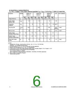
where:
APPLICATIONS AND DESIGN NOTES
VIN MAX = Maximum input voltage desired
(full count voltage)
= Integrating Resistor value
Determination and Selection of System Variables
RINT
Theprocedureoutlinedbelowallowstheusertodeterminethe
values for the following ALD500RAU/ALD500RA/ALD500R
system design variables:
For minimum noise and maximum linearity, RINT should be in
the range of between 50kΩ to 150kΩ .
Integrating Capacitor (CINT
)
(1) Determine Input Voltage Range
(2) Clock Frequency and Resolution Selection
(3) Input Integration Phase Timing
(4) Integrator Timing Components (RINT, CINT
(5) Auto Zero and Reference Capacitors
(6) Voltage Reference
The integrating capacitor should be selected to maximize
integrator output voltage swing VINT, for a given integration
time, without output level saturation. For +/-5V supplies,
recommended VINT range is between +/- 3 Volt to +/-4 Volt.
Using the 20µA buffer maximum output current, the value of
the integrating capacitor is calculated as follows:
)
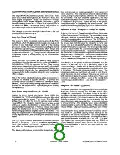
System Timing
-6
.
CINT = (tINT) (20 x 10 ) / VINT
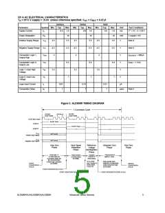
Figure 3 and Figure 4 show the overall timing for a typical
system in which ALD500RAU/ALD500RA/ALD500R is
interfaced to a microcontroller. The microcontroller drives the
A, B inputs with I/O lines and monitors the comparator output,
COUT, using an I/O line or dedicated timer-capture control pin.
It may be necessary to monitor the state of the comparator
output in addition to having it control a timer directly during the
Reference Deintegration Phase.
where: tINT
VINT
=
=
Input Integration Phase Period
Maximum integrator output
voltage swing
It is critical that the integrating capacitor must have a very low
dielectricabsorption, aschargelossorgainduringconversion
directlyconvertsintoanerrorvoltage. Polypropylenecapacitors
are recommended while Polyester and Polybicarbonate
capacitors may also be used in less critical applications.
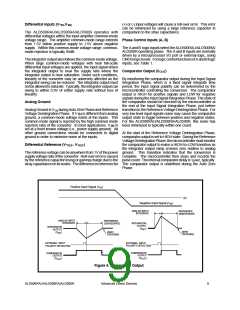
There are four critical timing events: sampling the input
polarity;capturingthedeintegrationtime;minimizingovershoot
and properly executing the Integrator Output Zero Phase.
Reference (CREF) and Auto Zero (CAZ) Capacitors
Selecting Input Integration Time
CREF and CAZ must be low leakage capacitors (e.g.
polypropylene types). The slower the conversion rate, the
larger the value CREF must be. Recommended capacitor
values for CREF and CAZ are equal to CINT. Larger values for
CAZ and CREF may also be used to limit roll-over errors.
For maximum 50/60 cycle noise rejection, Input Integration
Time must be picked as a multiple of the period of line
frequency. For example, tINT times of 33msec, 66msec and
100 msec maximize 60Hz line rejection, and 20msec, 40
msec, 80msec, and 100 msec maximize 50Hz line rejection.
Note that tINT of 100 msec maximizes both 60 Hz and 50Hz
line rejection.
Calculate VREF
The reference deintegration voltage is calculated using:
.
.
VREF = (VINT) (CINT) (RINT) / 2(tINT
)
INT and DINT Phase Timing
The ALD500RAU/ALD500RA/ALD500R requires an external
in order to operate properly. This R should be a 1%
metal film 100KΩ resistor, 50 ppm/C. Any other loading must
be high impedance (≥100MΩ).
The duration of the Reference Deintegrate Phase (DINT) is a
function of the amount of voltage charge stored on the
R
REF
REF
integrator capacitor during INT phase, and the value of VREF
.
The DINT phase must be initiated immediately following INT
phaseandterminatedwhenanintegratoroutputzero-crossing
is detected. In general, the maximum number of counts
chosenforDINT phaseistwicetothreetimesthatofINTphase
with VREF chosen as a maximum voltage relative to VIN. For
example, VREF = VIN(max)/2 would be a good reference
voltage.
Converter Noise
The converter noise is the total algebraic sum of the integrator
noise and the comparator noise. This value is typically 14 µV
peak to peak. The higher the value of the reference voltage,
the lower the converter noise. Such sources of noise errors
canbereducedbyincreasedintegrationtimes,whicheffectively
filter out any such noise. If the integration time periods are
selected as multiples of 50/60Hz frequencies, then 50/60Hz
noise is also rejected, or averaged out. The signal-to-noise
ratio is related to the integration time (tINT) and the integration
time constant (RINT) (CINT) as follows:
Integrating Resistor (RINT
)
The desired full-scale input voltage and amplifier output
current capability determine the value of RINT. The buffer and
integrator amplifiers each have a full-scale current of 20µA.
The value of RINT is therefore directly calculated as follows:
-6
.
.
S/N (dB) = 20 Log ((VINT / 14 x 10 ) tINT /(RINT CINT))
RINT
= VIN MAX / 20 µA
This converter noise can also be reduced by using multiple
samples and mathematically averaged. For example, taking
16samplesandaveragingthereadingsresultinamathematical
(by software) filtering of noise to less than 4µV.
10
Advanced Linear Devices
ALD500RAU/ALD500RA/ALD500R

 ALD [ ADVANCED LINEAR DEVICES ]