e. Very high resolution, high accuracy measurements
can be achieved simply and at very low cost.
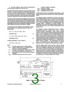
reference voltage is integrated
VREF = Reference Voltage
CINT = Integrating Capacitor value
RINT = Integrating Resistor value
Aninherentbenefitofthedualslopeconvertersystemisnoise
immunity. The input noise spikes are integrated (averaged to
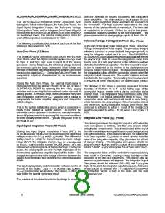
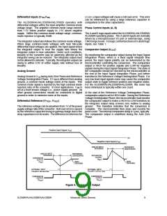
near zero) during the integration periods. Integrating ADCs Actual data conversion is accomplished in two phases: Input
are immune to the large conversion errors that plague SignalIntegrationPhaseandReferenceVoltageDeintegration
successiveapproximationconvertersandotherhighresolution Phase.
converters and perform very well in high-noise environments.
The integrator output is initialized to 0V prior to the start of
Theslowconversionspeedoftheintegratingconverterprovides InputSignalIntegrationPhase. DuringInputSignalIntegration
inherentnoiserejectionwithatleasta20dB/decadeattenuation Phase, internal analog switches connect VIN to the buffer
rate. Interferencesignalswithfrequenciesatintegralmultiples input where it is maintained for a fixed integration time period
oftheintegrationperiodare,theoretically,completelyremoved. (tINT). This fixed integration period is generally determined by
Integrating converters often establish the integration period to a digital counter controlled by a crystal oscillator. The
reject 50/60Hz line frequency interference signals.
application of VIN causes the integrator output to depart 0V at
a rate determined by VIN and a direction determined by the
polarity of VIN.
The relationship of the integrate and deintegrate (charge
and discharge) of the integrating capacitor values are
shown below:
The Reference Voltage Deintegration Phase is initiated
immediately after tINT, within 1 clock cycle. During
ReferenceVoltage Deintegration Phase, internal analog
switchesconnectareferencevoltagehavingapolarityopposite
that of VIN to the integrator input. Simultaneously the same
digital counter controlled by the same crystal oscillator used
above is used to start counting clock pulses. The Reference
VoltageDeintegrationPhaseismaintaineduntilthecomparator
output inside the dual slope analog processor changes state,
indicating the integrator has returned to 0V. At that point the
digital counter is stopped. The Deintegration time period
(tDINT), as measured by the digital counter, is directly
proportional to the magnitude of the applied input voltage.
. .
tINT / RINT CINT)
VINT = VX - (VIN
(integrate cycle)
(1)
(2)
(3)
. .
tDINT / RINT CINT)
VX = VINT - (VREF
(deintegrate cycle)
Combining equations 1 and 2 results in:
IN / VREF = -tDINT / tINT
where:
V
After the digital counter value has been read, the digital
counter, the integrator, and the auto zero capacitor are all
reset to zero through an Integrator Zero Phase and an Auto
Zero Phase so that the next conversion can begin again. In
practice, this process is usually automated so that analog-to-
digital conversion is continuously updated. The digital control
Vx = An offset voltage used as starting voltage
VINT = Voltage change across CINT during tINT and
during tDINT (equal in magnitude)
VIN = Average, or an integrated, value of input voltage
to be measured during tINT (Constant VIN)
tINT = Fixed time period over which unknown voltage is ishandledbyamicroprocessororadedicatedlogiccontroller.
integrated
The output, in the form of a binary serial word, is read by a
microprocessor or a display adapter when desired.
tDINT = Unknown time period over which a known
C
INT
INTEGRATOR
-
R
INT
V
INT
COMPARATOR
-
C
ANALOG
INPUT
OUT
+
(V
)
IN
+
S1
POLARITY
DETECTION
PHASE
CONTROL
SWITCH DRIVER
POLARITY CONTROL
VOLTAGE
REFERENCE
REF
SWITCHES
CONTROL
LOGIC
A
B
V
= 4.1V MAX
INT
V
V
IN ≈ FULL SCALE
MICROCONTROLLER
(CONTROL LOGIC
+ COUNTER)
V
V
IN ≈ 1/2 FULL SCALE
V
x
≈
0
t
DINT
t
t
INT
DINT
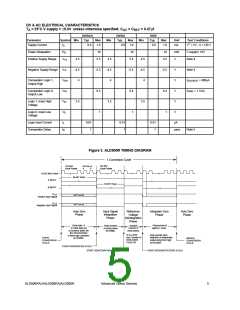
Figure 2. Basic Dual-Slope Converter
ALD500RAU/ALD500RA/ALD500R
Advanced Linear Devices
3

 ALD [ ADVANCED LINEAR DEVICES ]