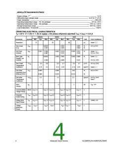
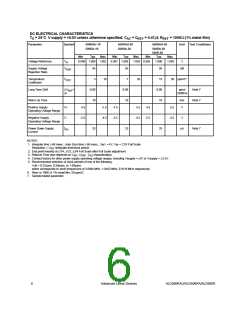
DC & AC ELECTRICAL CHARACTERISTICS
= 25°C V supply = ±5.0V unless otherwise specified; C = C = 0.47µf
REF
T
A
AZ
500RAU
Typ
500RA
Typ
500R
Typ
0.6
Parameter
Symbol Min
Max
Min
Max
Min
Max
Unit
Test Conditions
+
Supply Current
I
S
0.6
1.0
0.6
1.0
1.0
mA
V
= 5V , A =1,B=1
Power Dissipation
P
10
10
10
mW
V
V supply= ±5V
D
Positive Supply Range
V
+S
4.5
-4.5
4
5.5
4.5
-4.5
4
5.5
4.5
5.5
Note 4
Negative Supply Range
V
-S
-5.5
0.4
1
-5.5
0.4
1
-4.5
4
-5.5
0.4
1
V
V
V
V
V
Note 4
Comparator Logic 1,
Output High
V
OH
I
I
= 400µA
SOURCE
Comparator Logic 0,
Output Low
V
OL
= 1.1mA
SINK
Logic 1, Input High
Voltage
V
IH
3.5
3.5
3.5
Logic 0, Input Low
Voltage
V
IL
Logic Input Current
Comparator Delay
I
t
0.01
1
0.01
1
0.01
1
µA
L
µsec
Note 5
D
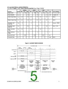
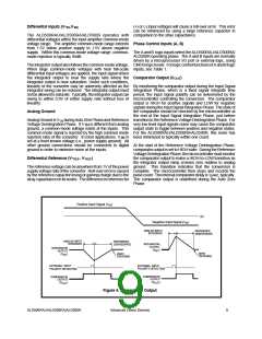
Figure 3. ALD500R TIMING DIAGRAM
1 Conversion Cycle
123,093
Clock Pulses
123,093
Clock Pulses
0.5416 µs
~
~
1.8432 MHz Clock
A INPUT
66.667 msec.
66.667 msec.
B INPUT
COUT
NOT VALID
NOT VALID
Positive Input Signal
COUT
Negative Input Signal
Auto Zero
Phase
Input Signal
Integration
Phase
Reference
Voltage
Deintegration
Phase
Integrator Zero
Phase
Auto Zero
Phase
Clock data in
or clock data out
of counters within the
the microcontroller
or fixed logic controller,
as needed.
Fixed period of
approx.1 msec.
Variable
number of
clock pulses.
Fixed number
of clock pulses
by design.
At VIN MAX,
max. number of
clock pulses
Stop counter upon
detection of comparator
output going from high
to low state.
START
REPEAT
CONVERSION
CYCLE
CONVERSION
CYCLE
~
= 246,185
START INTEGRATION CYCLE
START DEINTEGRATION CYCLE
START INTEGRATOR ZERO CYCLE
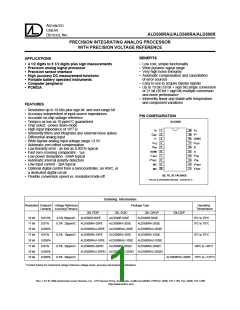
ALD500RAU/ALD500RA/ALD500R
Advanced Linear Devices
5

 ALD [ ADVANCED LINEAR DEVICES ]