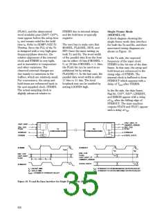
(FLAG), and the data/control
word available pins (DAV*, CAV*),
must appear before the setup time
ts, and remain valid for the hold
time th. Refer to HDMP-1022 Tx
Timing. Since the PLL of the Tx
is designed with a very high-gain
frequency/phase detector, the
relative alignment of the internal
clock and STRBIN is very tight,
and is insensitive to temperature
and other variations. The
observed external changes are
due mainly to variations in the
buffers, which are relatively small.
For convenience, the setup and
hold times are referenced back to
the user-supplied clock, STRBIN.
The actual sampling clock is
STRBIN due to internal delays,
and the hold time is typically
negative.
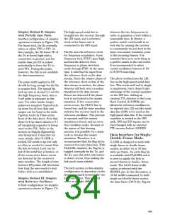
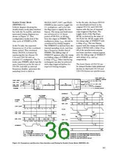
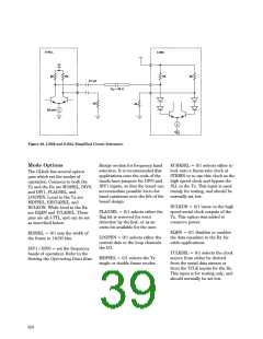
Single Frame Mode
(MDFSEL=0)
A block diagram showing the
single-frame mode data interface
for both the Tx and Rx, and their
associated timing diagrams are
shown in Figure 18.
The user has to make sure that
M20SEL, FLAGSEL, DIV0, and
DIV1 have the same setting on
both Tx and Rx. The word width
of the parallel data from the host
can be either 16 bits if M20SEL =
0, or 20 bits if M20SEL = 1. Also,
the FLAG bit can be used as an
additional bit by setting
FLAGSEL=1. In the last case, the
parallel data word width is either
17 bits or 21 bits. The local
loopback test can be enabled by
setting LOOPEN high.
In the Tx side, the expected
frequency of the input clock
STRBIN is the bit rate of the data
frame. In this case, the setup and
hold times are referenced to the
rising edge of STRBIN. The
internal clock is buffered to form
STRBOUT which appears with a
delay of Tstrb after STRBIN.
In the Rx side, the data frame,
flag bit, CAV*, DAV*, LINKRDY,
and ERROR appear with a delay
of td1 after the falling edge of
STRBOUT. The state machine
outputs STAT0 and STAT1 appear
with a delay of td2.
slightly advanced relative to
CAV*, DAV*, FF
LINKRDY, ERROR
D00 - D19
FLAG
CAV*, DAV*
D00 - D19
FLAG
Tx
CONFIGURATIONS
Rx
CONFIGURATIONS
STRBOUT
STRBIN
STRBOUT
STAT0, STAT1
PLL
STRBIN
STRBOUT
t
strb
t
t
d2
d1
D00 - D19
FLAG
CAV*, DAV*, FF
LINKRDY, ERROR
D00 - D19
CAV*, DAV*
FLAG
t
t
h
s
STAT0, STAT1
STRBOUT
t
t
t
= SETUP TIME
= HOLD TIME
t
t
= STRBOUT TO SYNCHRONOUS OUTPUTS DELAY
= STRBOUT TO STATE MACHINE OUTPUTS DELAY
s
h
d1
d2
= STRBIN TO STRBOUT DELAY
strb
Figure 18. Tx and Rx Data Interface for Single Frame Mode (MDFSEL=0).
650

 AGILENT [ AGILENT TECHNOLOGIES, LTD. ]