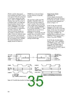
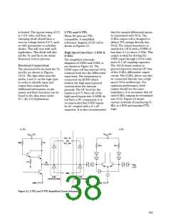
Double Frame Mode
(MDFSEL=1)
In the Rx side, the frame D0-D19
are demultiplexed back to the
original C0-C19, and C20-C39
frames with the use of external
edge-triggered flip-flops. The
toggle clock of the flip-flops,
RCLK, is derived by the state of
the FLAG bit. RCLK toggle with
the rising edge of STRBOUT with
a delay of tda. The two frames
appear with the rising and falling
edges of RCLK with a delay of tdb.
All of the synchronous outputs
and state machine outputs appear
after the falling edge of STRBOUT
with delays of td1 and td2
D0-D19, DAV*, CAV*, and FLAG.
STRBIN is also used to toggle the
2:1 multiplexer, and is fed into
the flag input to signify the two
frames. The setup and hold times
are referenced to 1/2 frame
period of D0-D19, or 90 deg,
from the edges of STRBIN. The
multiplexer delay, tmux, should be
considered for timing margins.
The STRBOUT is derived from the
internal sampling clock, and thus
has a frequency double that of
STRBIN. The falling edge of
STRBOUT appears after the rising
and falling edges of STRBIN after
a delay of Tstrb. Other interlacing
techniques can also be achieved
with edge-triggered latches for
improved timing margins.
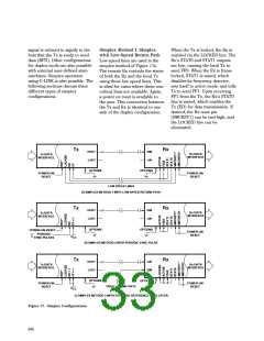
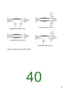
A block diagram showing the
double-frame mode data interface
for both the Tx and Rx, and their
associated timing diagrams are
shown in Figure 17. This
configuration works best if the
duty cycle of STRBIN is 50%.
In the Tx side, the expected
frequency is 1/2 of the combined
frame period. This combined
frame, D0-D19, is formed by
interlacing the two frames C0-
C19 and C20-C39 with an
external 2:1 multiplexer. The Tx
locks onto STRBIN, which has the
same frequency as the bit rate of
C0-C39, and with an internal
frequency doubler, generates the
sampling clock to latch in
respectively.
The lower frame of C0-C19 can
be delayed further with additional
latches so that both C0-C19 and
C20-C39 frames are synchronous.
CAV*, DAV*, FF
LINKRDY, ERROR
C00 - C19
CAV*, DAV*
D00 - D19
0
D00 - D19
C00 - C19
2:1
MUX
1
Tx
Rx
C20 - C39
FLAG
FLAG
C20 - C39
STRBOUT
CONFIGURATIONS
CONFIGURATIONS
RCLK
STRBOUT
STRBIN
STAT0; STAT1
PLL
STRBOUT
1/2 FRAME
PERIOD
1/2 FRAME
PERIOD
t
t
d2
d1
CAV*, DAV*
FF, LINKRDY
ERROR
STRBIN
FLAG
D00 - D19
C00 - C19
C20 - C39
CAV*, DAV*
t
t
t
t
t
t
h
s
h
s
FLAG
t
t
da
C00 - C19
C20 - C39
da
RCLK
t
t
strb
mux
t
t
db
db
D00 - D19
STRBOUT
C00 - C19
C20 - C39
C00 - C19
C20 - C39
t
t
h
s
h
s
STAT0
STAT1
t
t
t
t
= SETUP TIME
= HOLD TIME
s
h
t
t
t
t
= STRBOUT TO SYNCHRONOUS OUTPUTS DELAY
= STRBOUT TO STATE MACHINE OUTPUTS DELAY
= STRBOUT TO RCLK DELAY
= STRBIN TO STRBOUT DELAY
= 2:1 MULTIPLEXER DELAY
d1
d2
da
db
strb
mux
= RCLK TO C00-C39 OUTPUT DELAY
Figure 19. Transmitter and Receiver Data Interface and Timing for Double Frame Mode (MDFSEL=0).
651

 AGILENT [ AGILENT TECHNOLOGIES, LTD. ]