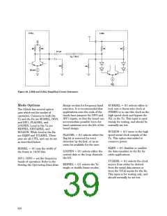
O-BLL
I-H50
12
80
80
50
50
0.1 µF
Z
= 50 Ω
O
50
50
28 mA
V
EE
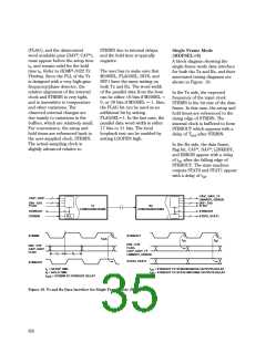
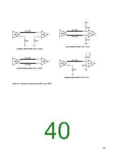
Figure 22. I-H50 and O-BLL Simplified Circuit Schematic.
Mode Options
Range section for frequencyband
selection. It is recommended that
applications near the ends of the
bands have jumpers for DIV0 and
DIV1 inputs, so that the board can
accommodate possible lot-to-lot
band variations over the life of the
board design.
ECHKSEL = 0/1 selects either to
lock onto a frame-rate clock at
STRBIN or to use this clock as the
high speed clock and bypass the
PLL in the Tx. This input is used
mainly for testing, and should be
normally set low.
The GLlink has several option
pins which set the modes of
operation. Common to both the
Tx and the Rx are M20SEL, DIV0,
and DIV1, FLAGSEL, and
LOOPEN. Local to the Tx are
MDFSEL, EHCLKSEL, and
HCLKON. While local to the Rx
are EQEN and TCLKSEL. These
pins are all I-TTL, and can be set
as described below.
HCLKON = 0/1 turns on the high
speed serial clock outputs of the
Tx. This option was added to
conserve power.
FLAGSEL = 0/1 selects either the
flag bit is reserved for error
detection by the link, or as an
extra bit available for the user.
EQEN = 0/1 disables or enables
the data equalizer in the Rx for
cable applications.
M20SEL = 0/1 sets the width of
the frame to 16/20 bits.
LOOPEN = 0/1 selects either the
normal data or the loop channels
the I/O.
DIV1 / DIV0 = set the frequency
bands of operation. Refer to the
Setting the Operating Data Rate
TCLKSEL = 0/1 selects the clock
source from either be derived
from the serial data stream or
from the TCLK inputs for the Rx.
This input is for testing only, and
should normally be set low.
MDFSEL = 0/1 selects the Tx
single or double frame modes.
654

 AGILENT [ AGILENT TECHNOLOGIES, LTD. ]