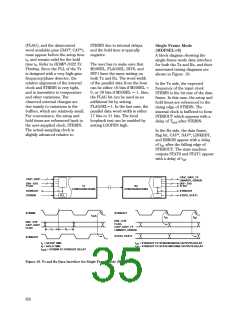
Supply Bypassing and
Integrator Capacitor
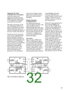
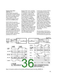
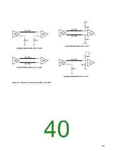
Figure 20 shows the location of
the PLL integrator capacitors,
power supply capacitors and
required grounding for the Tx and
Rx chips.
R1
C1
CAP0B
CAP0A
CAP1A
CAP1B
C2
D1
HP
HDMP-1022
Integrating Capacitor
LOT#
Tx
The integrating capacitors (C2)
are required by both the Tx and
Rx to function properly. These
caps are used by the PLL for
frequency and phase lock and
directly set the stability and
lockup times. The designed value
of C2 is 0.1 µF, with a tolerance
of ± 10%. The internal charging
currents are scaled with the DIV0
and DIV1 settings such that the
same capacitor value works with
all four frequency bands. Larger
values of C2 improve jitter
DATECODE
C1
R1
C1
R1
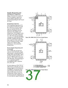
Figure 20a. HDMP-1022 (Tx) Power Supply Bypass.
R1
C1
performance, but extend the
lockup times.
D1
C2
Power Supply Bypassing and
Grounding
HP
HDMP-1024
R2
The G-LINK chip set has been
tested to work well with a single
ground plane, assuming that it is
a fairly clean ground plane. Thus,
all of the separate grounds (VCC,
and VCC_TTL) can be connected
onto this plane. The bypassing of
VCC to ground should be
LOT#
Rx
DATECODE
C1
R1
C1
R1
accomplished with a capacitor
(C1) of 0.1 µF.
R2
C1 = BYPASS CAPACITOR
C2 = PLL INTEGRATOR CAPACITOR
D1 = OPTIONAL CLAMPING DIODE
0.1 µF
0.1 µF
In some instances, if the VCO of
either the Tx or the Rx are at the
extreme high end, the frequency
of STRBOUT exceeds the maxi-
mum frequency allowed by the
hosts. In this case, it is recom-
mended that a diode clamp, D1,
be used across the integrating cap
C2, such that the upper frequency
Figure 20b. HDMP-1022 (Rx) Power Supply Bypass.
652

 AGILENT [ AGILENT TECHNOLOGIES, LTD. ]