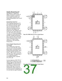
is limited. The typical swing of C2
is ± 0.8 volts, and thus, the
that the unused differential inputs
be terminated with 50 Ω. The
O-BLL output cell is designed to
deliver TTL swings directly into
50 Ω. The output impedance is
matched to 50 Ω with a VSWR of
less than 2:1 to above 2 GHz. This
output is ideal for driving the
I-H50 input through a 50 Ω cable
and a 0.1 uF coupling capacitor.
The 150 Ω shunt resistor to
ground improves internal DC bias
of the O-BLL differential output
circuit. The O-BLL driver can also
be connected directly into a high
speed 50 Ω oscilloscope. For
optimum performance, both
output should see the same
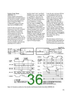
I-TTL and O-TTL
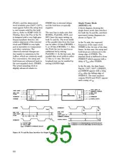
These I/O pins are TTL-
compatible. A simplified
schematic diagram of I/O cell is
shown in Figures 21.
clamping diode should have a
turn-on voltage below 0.8 V, such
as with germanium or schottky
diodes. This will vary with each
application. This diode will also
aid the Tx and Rx in the initial
frequency lock-in process.
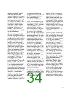
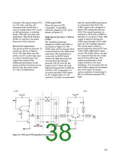
High Speed Interface: I-H50 &
O-BLL
The simplified schematic
diagrams of I-H50 and O-BLL is
are shown in Figure 22. The
I-H50 input cell has internal 50 Ω
resistors built into the differential
input lines. The termination is
connected via HGND which
isolates the high speed ground
currents from the internal
grounds. The DC level for the
inputs is at 0 V. Since all of the
high speed inputs into G-LINK do
not have a DC component, it is
recommended that I-H50 inputs
be AC coupled with a 0.1 µF
capacitor. It is also recommended
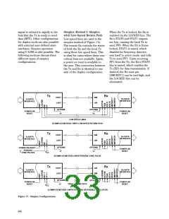
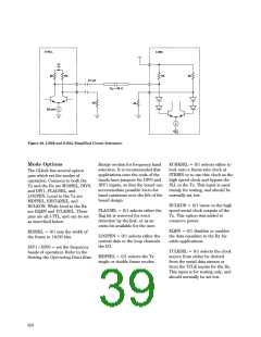
Electrical Connections
The electrical I/Os for both the Tx
and Rx are shown in Figures
19-21. The data sheet uses the
prefix, I and O, on the logic type
in order to identify input and
output lines respectively.
Additional information on pin
names and their functions can be
found in the data sheet under
Tx / Rx I/O Definitions.
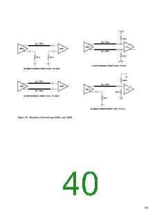
impedance. It is necessary that all
used O-BLL outputs be terminated
into 50 Ω. Figure 23 shows
various methods of interfacing O-
BLL to I-H50 and standard TTL
logic.
O_TTL
I_TTL
V
_TTL
CC
V
_TTL
CC
V
_Tx
CC
OR
800
72
V
_Rx
CC
10 k
10 k
6 k
36
V
BB
1.4 V
GND
ESD
ESD
PROTECTION
PROTECTION
GND_TTL
GND_TTL
Figure 21. I-TTL and O-TTL Simplified Circuit Schematic.
653

 AGILENT [ AGILENT TECHNOLOGIES, LTD. ]